CXA2055P 查看數據表(PDF) - Sony Semiconductor
零件编号
产品描述 (功能)
生产厂家
CXA2055P Datasheet PDF : 20 Pages
| |||
CXA2055P
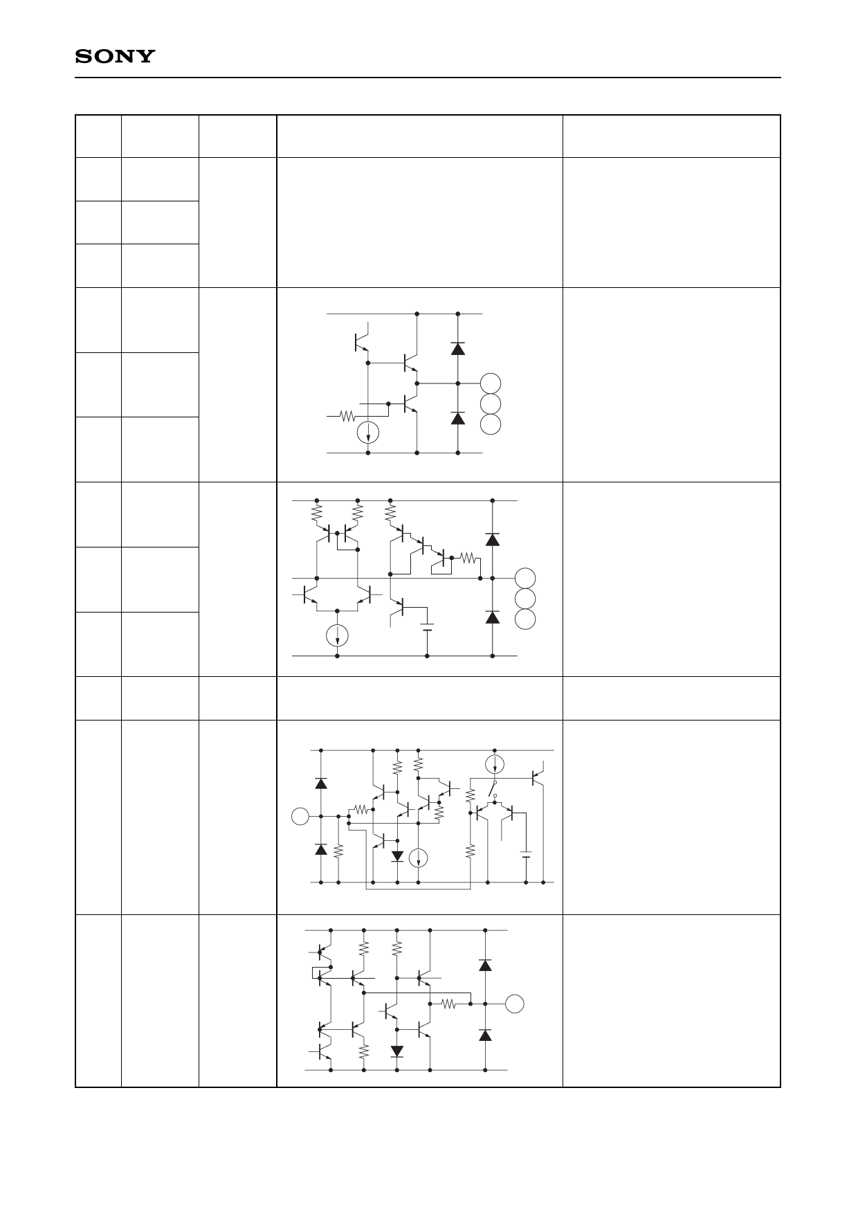
Pin
Symbol
No.
17 GND-B
Pin
voltage
21 GND-G
0V
24 GND-R
18 B-OUT
Equivalent circuit
Description
R, G and B independent GND.
VCC1
22 G-OUT
—
200
25 R-OUT
18
22
25
GND
R, G and B outputs.
19 B-S/H
23 G-S/H
—
26 R-S/H
21 VCC1
12 V
DA
27 /CSYNC
/ABL
VDET
28
—
/COF-RGB
1k 1k
1k
1k
225µA
2.5V
VCC2
27
GND
5k
100
100k
100
4k
50k
7.4k
100 5k
100
100
—5—
VCC1
Connection for external sample-
19
23
and-hold capacitor (0.1 µF).
26
GND
12 V power supply.
General-purpose D/A converter
output. Composite sync output.
TTL drive is possible.
1V
VL=0.5 V or less, VH=4.0 V or more
RGB output amplitude gain
compensation input.
(common for all three channels)
Function switching is performed
via the I2C bus.
VCC2
Video signal detection output.
VL=0.5 V or less, VH=4.0 V or more
General-purpose D/A converter
28
output.
The variable range is 1 to 4 V.
Function switching is performed
GND
via the I2C bus.
Share Link: 