MXL1001 查看數據表(PDF) - Maxim Integrated
零件编号
产品描述 (功能)
生产厂家
MXL1001 Datasheet PDF : 4 Pages
| |||
Precision Operational Amplifier
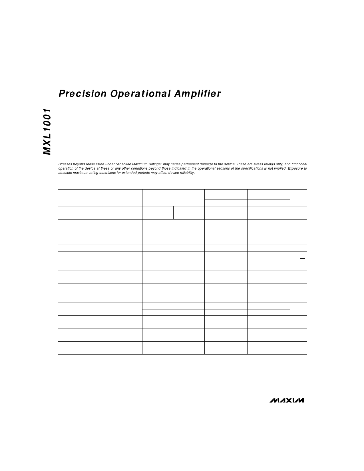
ABSOLUTE MAXIMUM RATINGS
Total Supply Voltage (V+ to V-) ...........................................±22V
Continuous Power Dissipation .........................................500mW
TO-99(H)—derate at 7.1mW/°C above +80°C
CERDIP(J)—derate at 6.7mW/°C above +75°C
Plastic DIP(P)—derate at 5.6mW/°C above +36°C
Small Outline(S)—derate at 5mW/°C above +55°C
Differential Input Voltage .....................................................±30V
Input Voltage (Note 1)..........................................................±22V
Duration of Output Short Circuit ....................................Indefinite
Operating Temperature Ranges:
MXL1001C_/AC_.................................................0°C to +70°C
MXL1001M_/AM_...........................................-55°C to +125°C
Junction Temperature (TJ).................................-65°C to +160°C
Storage Temperature Range .............................-65°C to +150°C
Lead Temperature (soldering, 10sec) .............................+300°C
Note 1: For supply voltages less than ±22V, the absolute maximum input voltage is equal to the supply voltage.
Stresses beyond those listed under “Absolute Maximum Ratings” may cause permanent damage to the device. These are stress ratings only, and functional
operation of the device at these or any other conditions beyond those indicated in the operational sections of the specifications is not implied. Exposure to
absolute maximum rating conditions for extended periods may affect device reliability.
ELECTRICAL CHARACTERISTICS
(VS = ±15V, TA = +25°C, unless otherwise noted.)
PARAMETER
SYMBOL
CONDITIONS
MXL1001AM
MXL1001AC
MIN TYP MAX
MXL1001M
MXL1001C
UNITS
MIN TYP MAX
Input Offset Voltage
VOS (Note 2)
MXL1001AM
MXL1001AC
7 15
10 25
18 60
µV
18 60
Long-Term Input Offset
Voltage Stability
VOS/Time (Note 3)
0.2 1.0
0.3
1.5
µV/
Month
Input Offset Current
Input Bias Current
Input Noise Voltage
Input Noise Voltage Density
Input Resistance
(Differential Mode)
IOS
IB
eN p-p
eN
RIN
0.1Hz to 10Hz (Note 4)
fO = 10Hz (Note 4)
fO = 100Hz (Note 4)
fO = 1000Hz (Note 4)
(Note 5)
0.3
±0.5
0.3
10.3
10.0
9.6
2.0
±2.0
0.6
18.0
13.0
11.0
30 100
0.4
±0.7
0.3
10.5
10.0
9.8
3.8
±4.0
0.6
18.0
13.0
11.0
nA
nA
µVp-p
nV/√Hz
15 80
MΩ
Input Voltage Range
Common-Mode Rejection Ratio
Power-Supply Rejection Ratio
Large-Signal Voltage Gain
Output Voltage Swing
Slew Rate
Closed-Loop Bandwidth
Power Consumption
IVR
CMRR
PSRR
AVO
VO
SR
BW
PD
VCM = ±13V
VS = ±3V to ±18V
RL ≥ 2kΩ, VO = ±12V
RL ≥ 1kΩ, VO = ±10V
RL ≥ 2kΩ
RL ≥ 1kΩ
RL ≥ 2kΩ (Note 4)
AVCL = +1V (Note 4)
VS = ±15V, no load
VS = ±3V, no load
±13 ±14
114 126
110 123
450 800
300 500
±13.0 ±14.0
±12.0 ±13.5
0.1 0.25
0.4 0.8
46 75
4
6
±13 ±14
110 126
106 123
400 800
250 500
±13.0 ±14.0
±12.0 ±13.5
0.1 0.25
0.4 0.8
48 80
4
8
V
dB
dB
V/mV
V
V/µs
MHz
mW
Note 2: MXL1001A grade VOS is measured one minute after application of power. For all other grades VOS is measured
approximately 0.5 seconds after application of power.
Note 3: Long-Term Input Offset Voltage Stability refers to the average trend line of VOS vs. Time over extended periods after the first
30 days of operation. Excluding the initial hour of operation, changes in VOS during the first 30 operating days are typically
2.5µV. Parameter is sample tested.
Note 4: Sample tested.
Note 5: Guaranteed by design.
2 _______________________________________________________________________________________
Share Link: 