AD744S 查看數據表(PDF) - Analog Devices
零件编号
产品描述 (功能)
生产厂家
AD744S Datasheet PDF : 12 Pages
| |||
AD744
Table II. Recommended Values of CCOMP vs. Various Load Conditions for the Circuits of
Figures 31 and 32.
Max
Slew
–3 dB
R1
R2
Gain
Gain
CLOAD CCOMP CLEAD Rate Bandwidth
(⍀)
(⍀)
Follower Inverter (pF)
(pF) (pF) (V/s) (MHz)
4.99 k 4.99 k
2
4.99 k 4.99 k
2
4.99 k 4.99 k
2
4.99 k 4.99 k
2
499 Ω 4.99 k
11
499 Ω 4.99 k
11
499 Ω 4.99 k
11
1
50
0
7
75
2.51
1
150
5
7
37
2.31
1
1000
20
–
14
1.2
1
>2000 25
–
12.52
1.0
10
270
0
–
75
1.2
10
390
2
–
50
0.85
10
1000
5
–
372
0.60
NOTES
1Bandwidth with CLEAD adjusted for minimum settling time.
2Into large capacitive loads the AD744’s 25 mA output current limit sets the slew rate of the amplifier, in V/ µs, equal to 0.025
amps divided by the value of CLOAD in µF. Slew rate is specified into rated max CLOAD except for cases marked 2, which are
specified with a 50 pF. load.
R1*
VIN
CLEAD*
+VS
R2*
1F
0.1F
AD744
VOUT
*SEE TABLE II –VS
OPTIONAL
CCOMP
1F
0.1F
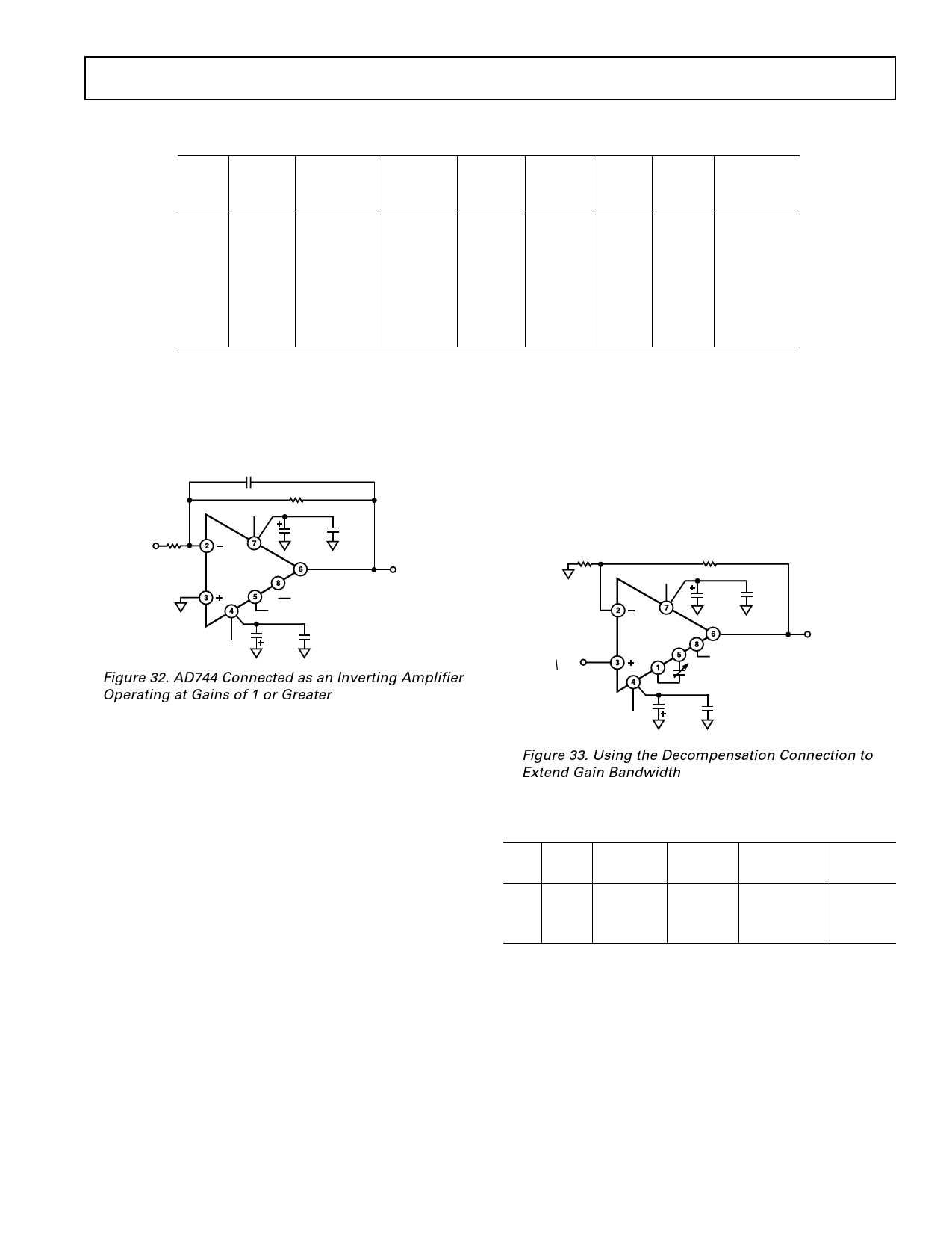
Figure 32. AD744 Connected as an Inverting Amplifier
Operating at Gains of 1 or Greater
Using Decompensation to Extend the Gain Bandwidth
Product
When the AD744 is used in applications where the closed-loop
gain is greater than 10, gain bandwidth product may be enhanced
by connecting a small capacitor between Pins 1 and 5 (Figure
33). At low frequencies, this capacitor cancels the effects of the
chip’s internal compensation capacitor, CCOMP, effectively dec-
ompensating the amplifier.
Due to manufacturing variations in the value of the internal
CCOMP, it is recommended that the amplifier’s response be
optimized for the desired gain by using a 2 to 10 pF trimmer
capacitor rather than using a fixed value.
R1*
R2*
+VS
1F
0.1F
\ VIN
AD744
VOUT
NOT CONNECTED
2 – 10pF
1F
–VS
*SEE TABLE III
0.1F
Figure 33. Using the Decompensation Connection to
Extend Gain Bandwidth
Table III. Performance Summary for the Circuit of Figure 33
R1 R2 Gain
Gain
–3 dB
Gain/BW
(⍀) (⍀) Follower Inverter Bandwidth Product
1 k 10 k 11
100 10 k 101
100 100 k 1001
10
100
1000
2.5 MHz
760 kHz
225 kHz
25 MHz
76 MHz
225 MHz
REV. C
–9–
Share Link: 