SN74LS193MR1 查看數據表(PDF) - ON Semiconductor
零件编号
产品描述 (功能)
生产厂家
SN74LS193MR1 Datasheet PDF : 8 Pages
| |||
SN74LS193
FUNCTIONAL DESCRIPTION
The LS193 is a 4-Bit Binary Synchronous UP / DOWN
(Reversable) Counter. Each circuit contains four
master/slave flip-flops, with internal gating and steering
logic to provide master reset, individual preset, count up and
count down operations.
Each flip-flop contains JK feedback from slave to master
such that a LOW-to-HIGH transition on its T input causes
the slave, and thus the Q output to change state. Synchronous
switching, as opposed to ripple counting, is achieved by
driving the steering gates of all stages from a common Count
Up line and a common Count Down line, thereby causing all
state changes to be initiated simultaneously. A
LOW-to-HIGH transition on the Count Up input will
advance the count by one; a similar transition on the Count
Down input will decrease the count by one. While counting
with one clock input, the other should be held HIGH.
Otherwise, the circuit will either count by twos or not at all,
depending on the state of the first flip-flop, which cannot
toggle as long as either Clock input is LOW.
The Terminal Count Up (TCU) and Terminal Count Down
(TCD) outputs are normally HIGH. When a circuit has
reached the maximum count state of 15, the next
HIGH-to-LOW transition of the Count Up Clock will cause
TCU to go LOW. TCU will stay LOW until CPU goes HIGH
again, thus effectively repeating the Count Up Clock, but
delayed by two gate delays. Similarly, the TCD output will
go LOW when the circuit is in the zero state and the Count
Down Clock goes LOW. Since the TC outputs repeat the
clock waveforms, they can be used as the clock input signals
to the next higher order circuit in a multistage counter.
Each circuit has an asynchronous parallel load capability
permitting the counter to be preset. When the Parallel Load
(PL) and the Master Reset (MR) inputs are LOW,
information present on the Parallel Data inputs (P0, P3) is
loaded into the counter and appears on the outputs regardless
of the conditions of the clock inputs. A HIGH signal on the
Master Reset input will disable the preset gates, override
both Clock inputs, and latch each Q output in the LOW state.
If one of the Clock inputs is LOW during and after a reset or
load operation, the next LOW-to-HIGH transition of that
Clock will be interpreted as a legitimate signal and will be
counted.
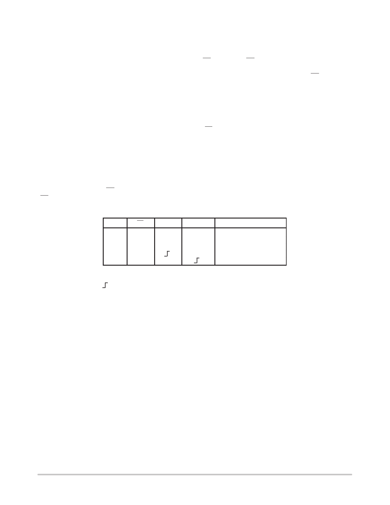
MODE SELECT TABLE
MR
PL
CPU
H
X
X
L
L
X
L
H
H
L
H
L
H
H
CPD
X
X
H
H
MODE
Reset (Asyn.)
Preset (Asyn.)
No Change
Count Up
Count Down
L = LOW Voltage Level
H = HIGH Voltage Level
X = Don’t Care
= LOW-to-HIGH Clock Transition
http://onsemi.com
4
Share Link: 