SL74HC192 查看數據表(PDF) - System Logic Semiconductor
零件编号
产品描述 (功能)
生产厂家
SL74HC192 Datasheet PDF : 7 Pages
| |||
SL74HC192
Presettable BCD/Decade UP/DOWN Counter
High-Performance Silicon-Gate CMOS
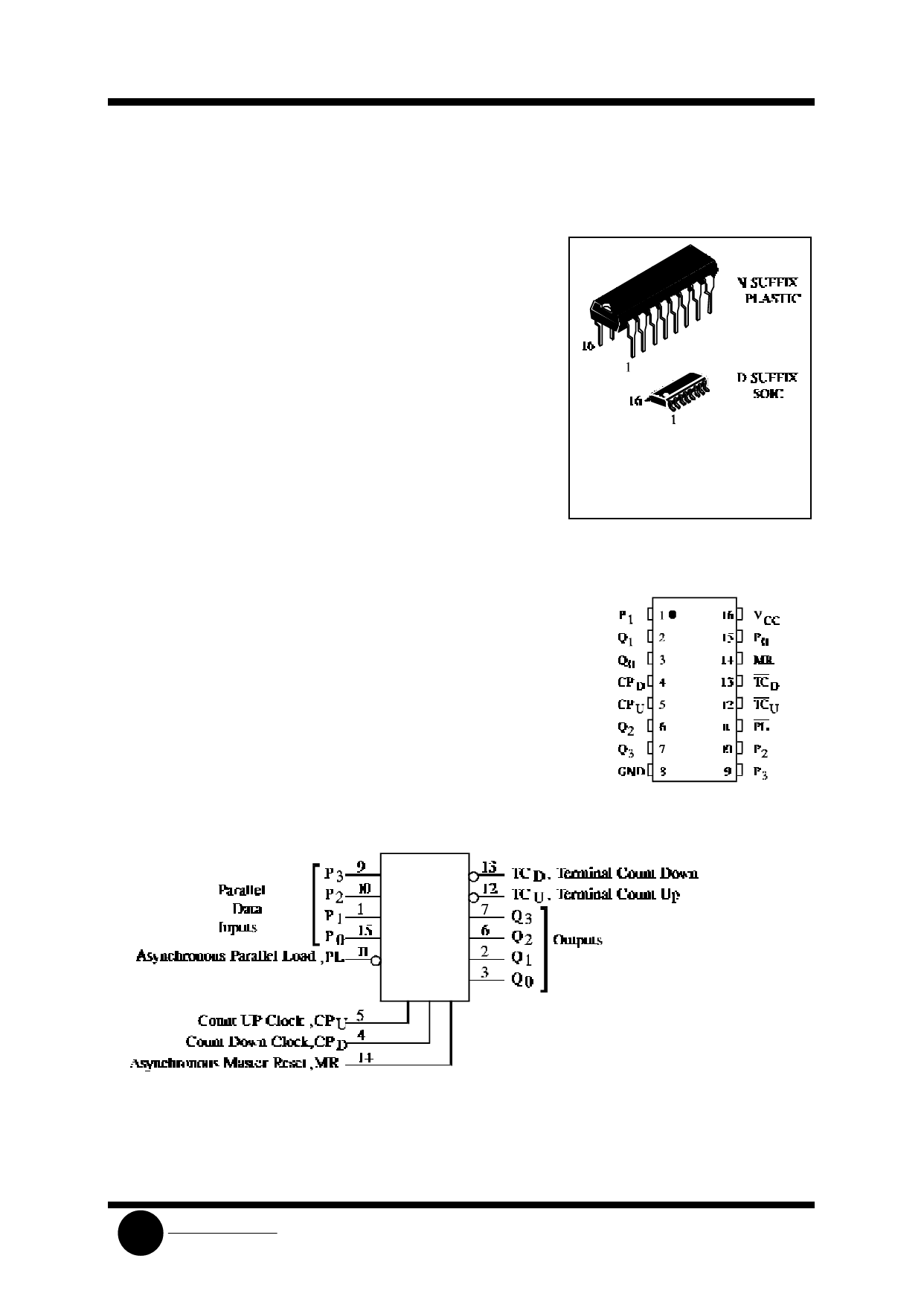
The SL74HC192 is identical in pinout to the LS/ALS192. The device
inputs are compatible with standard CMOS outputs; with pullup
resistors, they are compatible with LS/ALSTTL outputs.
The counter has two separate clock inputs, a Count Up Clock and
Count Down Clock inputs. The direction of counting is determined by
which input is clocked. The outputs change state synchronous with
the LOW-to-HIGH transitions on the clock inputs. This counter may be
preset by entering the desired data on the P0, P1, P2, P3 input. When
the Parallel Load input is taken low the data is loaded independently of
either clock input. This feature allows the counters to be used as
devide-by-n by modifying the count lenght with the preset inputs. In
addition the counter can also be cleared. This is accomplished by
inputting a high on the Master Reset input. All 4 internal stages are set
to low independently of either clock input.Both a Terminal Count
Down (TCD) and Terminal Count Up (TCU) Outputs are provided to
enable cascading of both up and down counting functions. The TCD
output produces a negative going pulse when the counter underflows
and TCU outputs a pulse when the counter overflows. The counter can
be cascaded by connecting the TCU and TCD outputs of one device to
the Count Up Clock and Count Down Clock inputs, respectively, of the
next device.
• Outputs Directly Interface to CMOS, NMOS, and TTL
• Operating Voltage Range: 2.0 to 6.0 V
• Low Input Current: 1.0 µA
• High Noise Immunity Characteristic of CMOS Devices
ORDERING INFORMATION
SL74HC192N Plastic
SL74HC192D SOIC
TA = -55° to 125° C for all packages
PIN ASSIGNMENT
LOGIC DIAGRAM
SLS
System Logic
Semiconductor
PIN 16 =VCC
PIN 8 = GND
Share Link: 