HCF4510BM013TR 查看數據表(PDF) - STMicroelectronics
零件编号
产品描述 (功能)
生产厂家
HCF4510BM013TR Datasheet PDF : 12 Pages
| |||
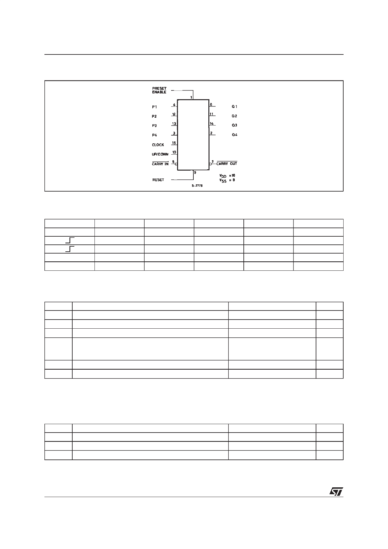
HCF4510B/4515B
FUNCTIONAL DIAGRAM
TRUTH TABLE
CL
X
X
X
X= Don’t care
CI
U/D
PE
1
X
0
0
1
0
0
0
0
X
X
1
X
X
X
R
Actio n
0
No Count
0
Count Up
0
Count Down
0
Preset
1
Reset
ABSOLUTE MAXIMUM RATING
Symbol
Parameter
Value
Unit
VDD * Supply Voltage
-0.5 to +18
V
Vi Input Voltage
-0.5 to VDD + 0.5
V
II DC Input Current (any one input)
± 10
mA
Ptot Total Power Dissipation (per package)
Dissipation per Output Transistor
200
mW
for Top = Full Package Temperature Range
100
mW
Top Operating Temperature
-40 to +85
oC
Tstg Storage Temperature
-65 to +150
oC
Stresses above those listedunder ”Absolute Maximum Ratings” may cause permanent damage to the device. This is a stress rating only and functional
operation ofthe device atthese or any other conditions above those indicated in the operational sections of this specification is not implied. Exposure to
absolute maximum ratingconditions for external periods may affect device reliability.
* Allvoltage values are referred to VSS pin voltage.
RECOMMENDED OPERATING CONDITIONS
Symbol
Parameter
VDD Supply Voltage
VI Input Voltage
Top Operating Temperature
Value
3 to 15
0 to VDD
-40 to +85
Unit
V
V
oC
2/12
Share Link: 