AD625SE 查看數據表(PDF) - Analog Devices
零件编号
产品描述 (功能)
生产厂家
AD625SE Datasheet PDF : 15 Pages
| |||
AD625
the I × R drops “inside the loop” and virtually eliminating this
error source.
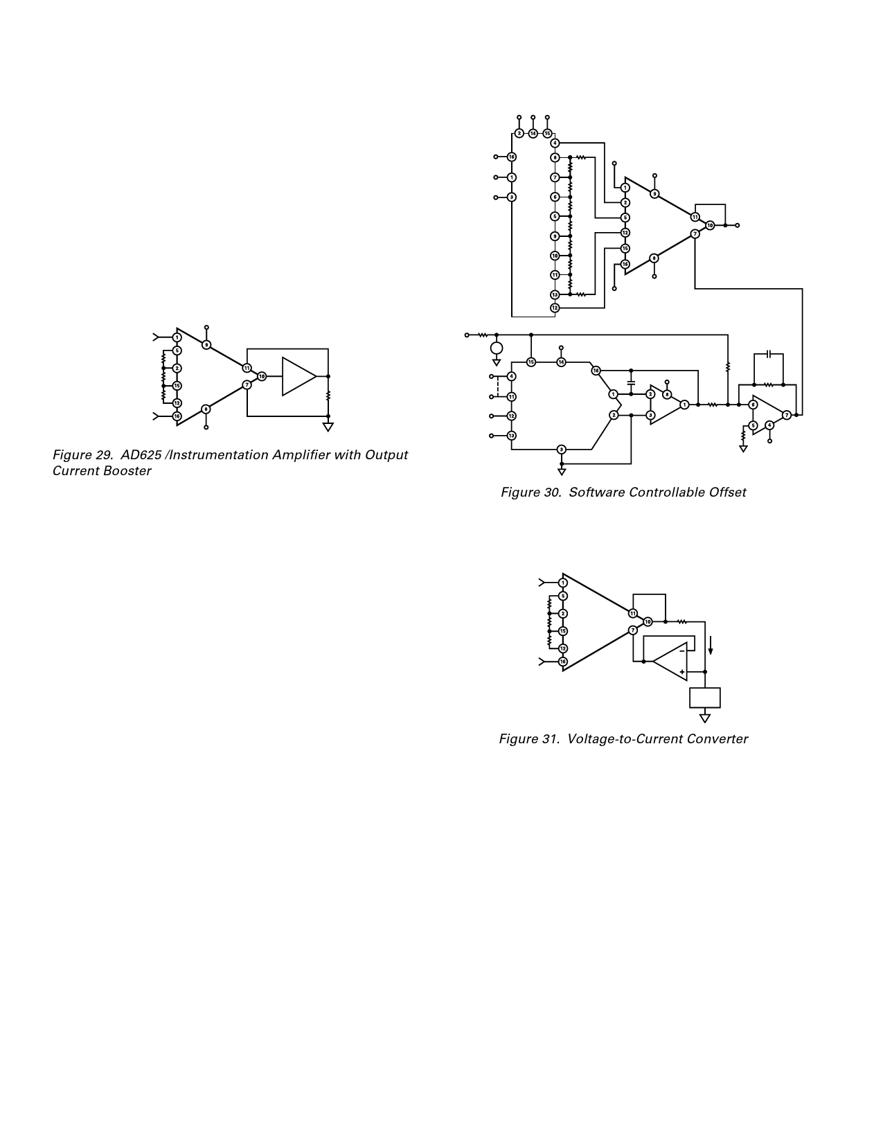
Typically, IC instrumentation amplifiers are rated for a full ± 10
volt output swing into 2 kΩ. In some applications, however, the
need exists to drive more current into heavier loads. Figure 29
shows how a high-current booster may be connected “inside the
loop” of an instrumentation amplifier. By using an external
power boosting circuit, the power dissipated by the AD625 will
remain low, thereby, minimizing the errors induced by self-
heating. The effects of nonlinearities, offset and gain inaccura-
cies of the buffer are reduced by the loop gain of the AD625’s
output amplifier.
VIN+
RF
RG
+VS
AD625
SENSE
X1
RF
RI
VIN–
–VS
REFERENCE
Figure 29. AD625 /Instrumentation Amplifier with Output
Current Booster
REFERENCE TERMINAL
The reference terminal may be used to offset the output by up
to ± 10 V. This is useful when the load is “floating” or does not
share a ground with the rest of the system. It also provides a
direct means of injecting a precise offset. However, it must be
remembered that the total output swing is ±10 volts, from
ground, to be shared between signal and reference offset.
The AD625 reference terminal must be presented with nearly
zero impedance. Any significant resistance, including those
caused by PC layouts or other connection techniques, will in-
crease the gain of the noninverting signal path, thereby, upset-
ting the common-mode rejection of the in-amp. Inadvertent
thermocouple connections created in the sense and reference
lines should also be avoided as they will directly affect the out-
put offset voltage and output offset voltage drift.
In the AD625 a reference source resistance will unbalance the
CMR trim by the ratio of 10 kΩ/RREF. For example, if the refer-
ence source impedance is 1 Ω, CMR will be reduced to 80 dB
(10 kΩ/1 Ω = 80 dB). An operational amplifier may be used to
provide the low impedance reference point as shown in Figure
30. The input offset voltage characteristics of that amplifier will
add directly to the output offset voltage performance of the
instrumentation amplifier.
The circuit of Figure 30 also shows a CMOS DAC operating in
the bipolar mode and connected to the reference terminal to
provide software controllable offset adjustments. The total offset
range is equal to ± (VREF/2 × R5/R4), however, to be symmetri-
cal about 0 V R3 = 2 × R4.
The offset per bit is equal to the total offset range divided by 2N,
where N = number of bits of the DAC. The range of offset for
Figure 30 is ± 120 mV, and the offset is incremented in steps of
0.9375 mV/LSB.
GND VDD VSS
A0
A1
EN
AD7502
+IN
+VS
AD625
SENSE
VOUT
VS 39k⍀
+VS
AD589 1.2V
MSB
DATA
INPUTS
LSB
CS
WR
AD7524
8-BIT DAC
–VS
–IN
REFERENCE
VREF
RFB
C1
OUT 1
OUT 2
R3
+VS
20k⍀
1/2
AD712
R4
10k⍀
5k⍀
0.01F
R5
2k⍀
1/2
AD712
–VS
Figure 30. Software Controllable Offset
An instrumentation amplifier can be turned into a voltage-to-
current converter by taking advantage of the sense and reference
terminals as shown in Figure 31.
VIN+
RF
RG
RF
VIN–
AD625
SENSE
+VX–
R1
IL
AD711
LOAD
Figure 31. Voltage-to-Current Converter
By establishing a reference at the “low” side of a current setting
resistor, an output current may be defined as a function of input
voltage, gain and the value of that resistor. Since only a small
current is demanded at the input of the buffer amplifier A1, the
forced current IL will largely flow through the load. Offset and
drift specifications of A2 must be added to the output offset and
drift specifications of the In-Amp.
INPUT AND OUTPUT OFFSET VOLTAGE
Offset voltage specifications are often considered a figure of
merit for instrumentation amplifiers. While initial offset may be
adjusted to zero, shifts in offset voltage due to temperature
variations will cause errors. Intelligent systems can often correct
for this factor with an autozero cycle, but this requires extra
circuitry.
–10–
REV. D
Share Link: 