AD625SE 查看數據表(PDF) - Analog Devices
零件编号
产品描述 (功能)
生产厂家
AD625SE Datasheet PDF : 15 Pages
| |||
AD625
Offset voltage and offset voltage drift each have two compo-
nents: input and output. Input offset is that component of offset
that is generated at the input stage. Measured at the output it is
directly proportional to gain, i.e., input offset as measured at the
output at G = 100 is 100 times greater than that measured at
G = 1. Output offset is generated at the output and is constant
for all gains.
The input offset and drift are multiplied by the gain, while the
output terms are independent of gain, therefore, input errors
dominate at high gains and output errors dominate at low gains.
The output offset voltage (and drift) is normally specified at
G = 1 (where input effects are insignificant), while input offset
(and drift) is given at a high gain (where output effects are negli-
gible). All input-related parameters are specified referred to the
input (RTI) which is to say that the effect on the output is “G”
times larger. Offset voltage vs. power supply is also specified as
an RTI error.
By separating these errors, one can evaluate the total error inde-
pendent of the gain. For a given gain, both errors can be com-
bined to give a total error referred to the input (RTI) or output
(RTO) by the following formula:
Total Error RTI = input error + (output error/gain)
Total Error RTO = (Gain × input error) + output error
The AD625 provides for both input and output offset voltage
adjustment. This simplifies nulling in very high precision appli-
cations and minimizes offset voltage effects in switched gain
applications. In such applications the input offset is adjusted
first at the highest programmed gain, then the output offset is
adjusted at G = 1. If only a single null is desired, the input offset
null should be used. The most additional drift when using only
the input offset null is 0.9 µV/°C, RTO.
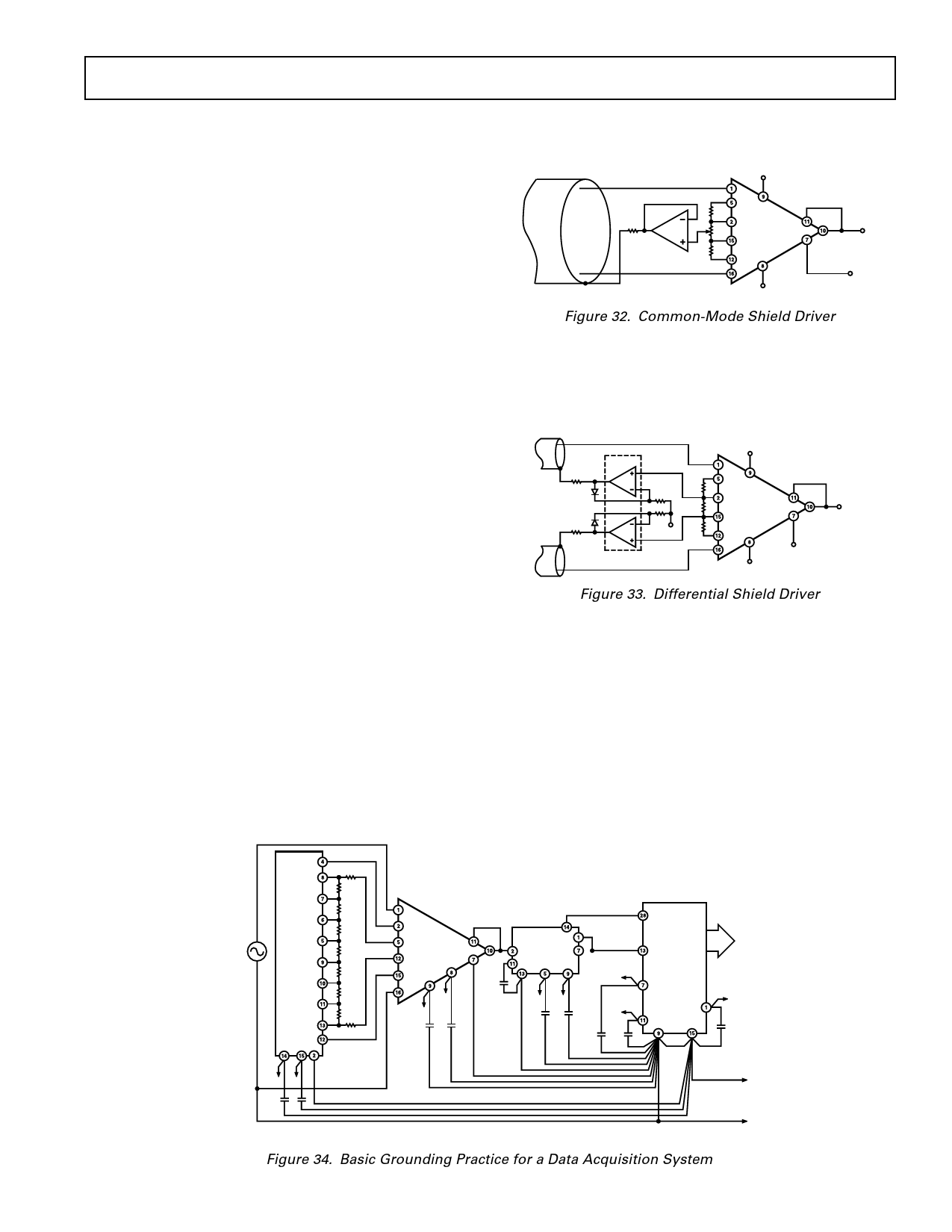
COMMON-MODE REJECTION
Common-mode rejection is a measure of the change in output
voltage when both inputs are changed by equal amounts. These
specifications are usually given for a full-range input voltage
change and a specified source imbalance.
In an instrumentation amplifier, degradation of common-mode
rejection is caused by a differential phase shift due to differences
in distributed stray capacitances. In many applications shielded
cables are used to minimize noise. This technique can create
+INPUT
100⍀
AD711
+VS
RF
RG AD625
RF
SENSE
VOUT
–INPUT
REFERENCE
–VS
Figure 32. Common-Mode Shield Driver
common-mode rejection errors unless the shield is properly
driven. Figures 32 and 33 show active data guards which are
configured to improve ac common-mode rejection by “boot-
strapping” the capacitances of the input cabling, thus minimiz-
ing differential phase shift.
100⍀
+INPUT
AD712
100⍀
RF
RG
–VS RF
+VS
AD625
SENSE
VOUT
REFERENCE
–INPUT
–VS
Figure 33. Differential Shield Driver
GROUNDING
In order to isolate low level analog signals from a noisy digital
environment, many data-acquisition components have two or
more ground pins. These grounds must eventually be tied to-
gether at one point. It would be convenient to use a single
ground line, however, current through ground wires and pc runs
of the circuit card can cause hundreds of millivolts of error.
Therefore, separate ground returns should be provided to mini-
mize the current flow from the sensitive points to the system
ground (see Figure 34). Since the AD625 output voltage is
developed with respect to the potential on the reference termi-
nal, it can solve many grounding problems.
REV. D
INPUT
SIGNAL
AD7502
AD625
–VS
+VS
HOLD
CAP
AD583
SAMPLE
AND
HOLD
–VS +VS
STATUS
ANALOG
OUT
+VS
AD574A
A/D
CONVERTER
–VS
VLOGIC
+VS –VS
DIGITAL
COMMON
ANALOG POWER
GROUND
Figure 34. Basic Grounding Practice for a Data Acquisition System
–11–
Share Link: 