AD625SE 查看數據表(PDF) - Analog Devices
零件编号
产品描述 (功能)
生产厂家
AD625SE Datasheet PDF : 15 Pages
| |||
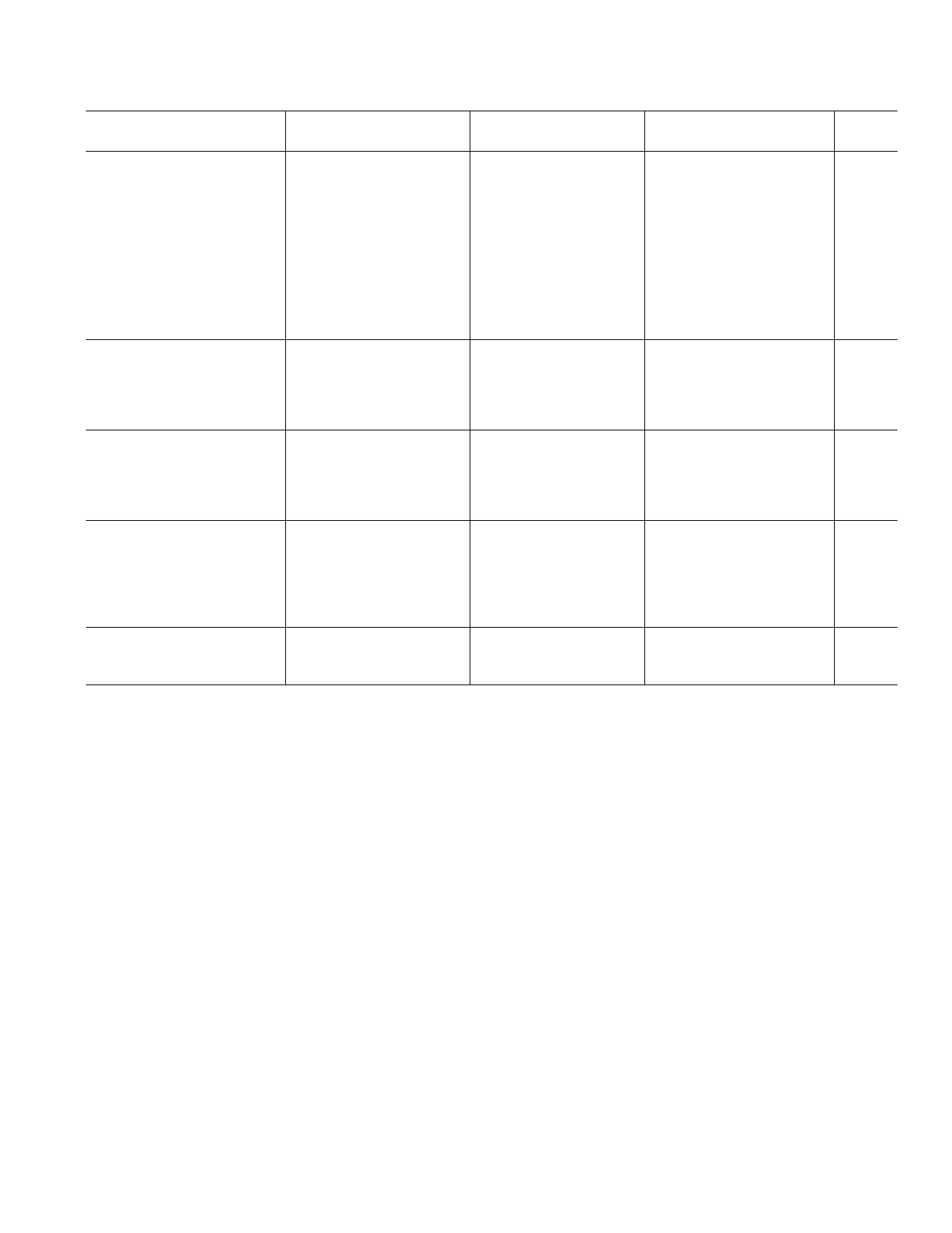
AD625
Model
AD625A/J/S
Min Typ
Max
AD625B/K
Min Typ Max
AD625C
Min Typ Max
Unit
NOISE
Voltage Noise, 1 kHz
R.T.I.
4
4
R.T.O.
75
75
R.T.I., 0.1 Hz to 10 Hz
G=1
10
10
G = 10
1.0
1.0
G = 100
0.3
0.3
G = 1000
0.2
0.2
Current Noise
0.1 Hz to 10 Hz
60
60
4
nV/√Hz
75
nV/√Hz
10
µV p-p
1.0
µV p-p
0.3
µV p-p
0.2
µV p-p
60
pA p-p
SENSE INPUT
RIN
IIN
Voltage Range
Gain to Output
10
30
± 10
1 ± 0.01
10
30
± 10
1 ± 0.01
10
kΩ
30
µA
± 10
V
1 ± 0.01
%
REFERENCE INPUT
RIN
IIN
Voltage Range
Gain to Output
20
30
± 10
1 ± 0.01
20
30
± 10
1 ± 0.01
20
kΩ
30
µA
± 10
V
1 ± 0.01
%
TEMPERATURE RANGE
Specified Performance
J/K Grades
0
A/B/C Grades
–40
S Grade
–55
Storage
–65
+70
0
+85
–40
+125
+150 –65
+70
+85
–40
+150
–65
°C
+85
°C
°C
+150
°C
POWER SUPPLY
Power Supply Range
Quiescent Current
± 6 to ± 18
3.5
5
± 6 to ± 18
3.5
5
± 6 to ± 18
V
3.5
5
mA
NOTES
1Gain Error and Gain TC are for the AD625 only. Resistor Network errors will add to the specified errors.
2VDL is the maximum differential input voltage at G = 1 for specified nonlinearity. VDL at other gains = 10 V/G. VD = actual differential input voltage.
Example: G = 10, VD = 0.50; VCM = 12 V – (10/2 × 0.50 V) = 9.5 V.
Specifications subject to change without notice.
All min and max specifications are guaranteed. Specifications shown in boldface are tested on all production units at final electrical test. Results from those tests are
used to calculate outgoing quality levels.
REV. D
–3–
Share Link: 