AD625SE 查看數據表(PDF) - Analog Devices
零件编号
产品描述 (功能)
生产厂家
AD625SE Datasheet PDF : 15 Pages
| |||
AD625
ABSOLUTE MAXIMUM RATINGS*
Supply Voltage . . . . . . . . . . . . . . . . . . . . . . . . . . . . . . . . . ± 18 V
Internal Power Dissipation . . . . . . . . . . . . . . . . . . . . . . 450 mW
Input Voltage . . . . . . . . . . . . . . . . . . . . . . . . . . . . . . . . . . . ± VS
Differential Input Voltage . . . . . . . . . . . . . . . . . . . . . . . . . ± VS
Output Short Circuit Duration . . . . . . . . . . . . . . . . Indefinite
Storage Temperature Range (D, E) . . . . . . . . –65°C to +150°C
Storage Temperature Range (N) . . . . . . . . . . –65°C to +125°C
Operating Temperature Range
AD625J/K . . . . . . . . . . . . . . . . . . . . . . . . . . . . 0°C to +70°C
AD625A/B/C . . . . . . . . . . . . . . . . . . . . . . . . –40°C to +85°C
AD625S . . . . . . . . . . . . . . . . . . . . . . . . . . . –55°C to +125°C
Lead Temperature Range (Soldering 10 sec) . . . . . . . . +300°C
*Stresses above those listed under Absolute Maximum Ratings may cause perma-
nent damage to the device. This is a stress rating only; functional operation of the
device at these or any other conditions above those indicated in the operational
section of this specification is not implied. Exposure to absolute maximum rating
conditions for extended periods may affect device reliability.
ORDERING GUIDE
Model
Temperature Range
AD625AD
AD625BD
AD625BD/+
AD625CD
AD625SD
AD625SD/883B
AD625SE/883B
AD625JN
AD625KN
AD625ACHIPS
AD625SCHIPS
5962-87719012A*
5962-8771901EA*
–40°C to +85°C
–40°C to +85°C
–40°C to +85°C
–40°C to +85°C
–55°C to +125°C
–55°C to +125°C
–55°C to +125°C
0°C to +70°C
0°C to +70°C
–40°C to +85°C
–55°C to +125°C
–55°C to +125°C
–55°C to +125°C
*Standard Military Drawing Available
Package Description
16-Lead Ceramic DIP
16-Lead Ceramic DIP
16-Lead Ceramic DIP
16-Lead Ceramic DIP
16-Lead Ceramic DIP
16-Lead Ceramic DIP
20-Terminal Leadless Chip Carrier
16-Lead Plastic DIP
16-Lead Plastic DIP
Die
Die
20-Terminal Leadless Chip Carrier
16-Lead Ceramic DIP
Package Option
D-16
D-16
D-16
D-16
D-16
D-16
E-20A
N-16
N-16
E-20A
D-16
CAUTION
ESD (electrostatic discharge) sensitive device. Electrostatic charges as high as 4000 V readily
accumulate on the human body and test equipment and can discharge without detection.
Although the AD625 features proprietary ESD protection circuitry, permanent damage may
occur on devices subjected to high-energy electrostatic discharges. Therefore, proper ESD
precautions are recommended to avoid performance degradation or loss of functionality.
WARNING!
ESD SENSITIVE DEVICE
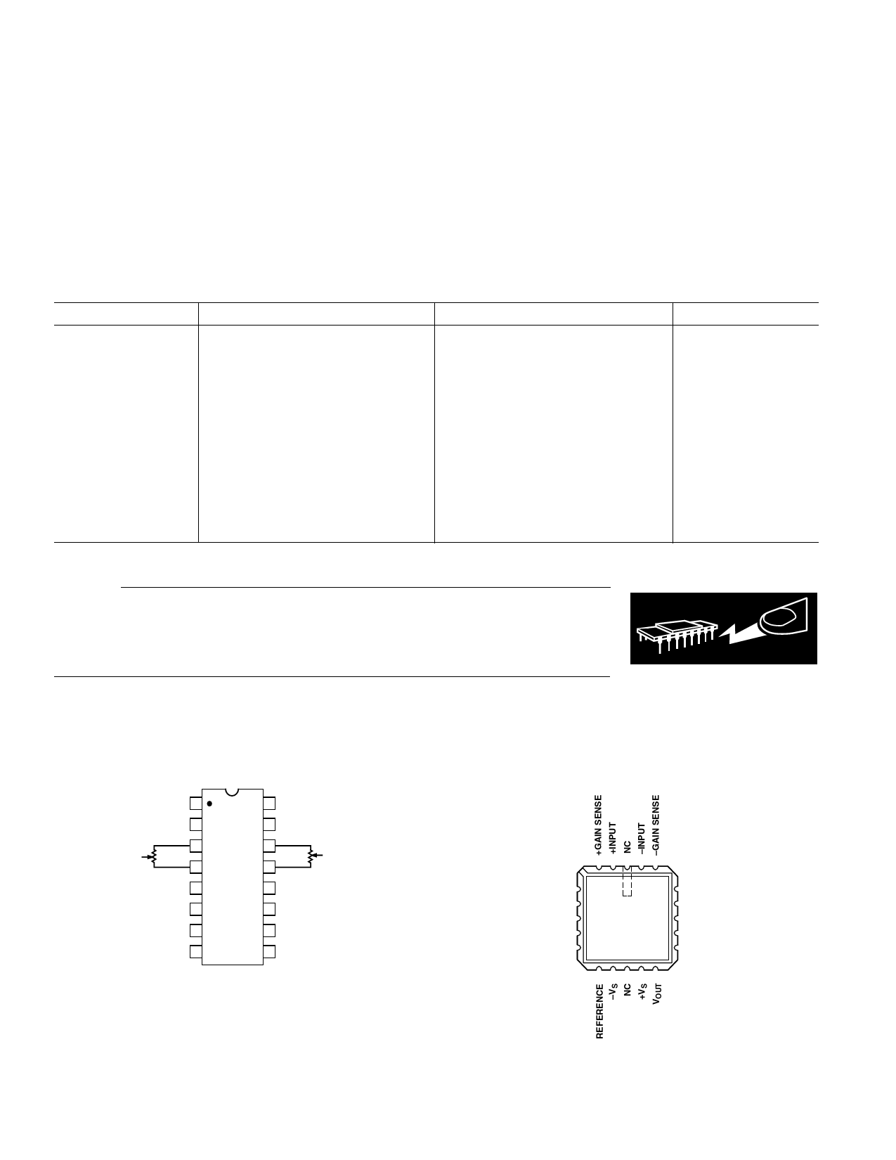
PIN CONNECTIONS
Ceramic DIP (D) and Plastic DIP (N) Packages
Leadless Chip Carrier (E) Package
+INPUT 1
16 –INPUT
+GAIN SENSE 2
15 –GAIN SENSE
RTI NULL
3
RTO NULL
14
+VS 10k⍀
10k⍀
–VS
4 AD625 13
RTI NULL
TOP VIEW
RTO NULL
+GAIN DRIVE 5 (Not to Scale) 12 –GAIN DRIVE
NC 6
11 SENSE
REFERENCE 7
–VS 8
10 VOUT
9 +VS
NC = NO CONNECT
3 2 1 20 19
RTI NULL 4
RTI NULL 5
NC 6
+GAIN DRIVE 7
NC 8
AD625
TOP VIEW
(Not to Scale)
18 RTO NULL
17 RTO NULL
16 NC
15 –GAIN NULL
14 SENSE
9 10 11 12 13
NC = NO CONNECT
–4–
REV. D
Share Link: 