MM1301AW 查看數據表(PDF) - Mitsumi
零件编号
产品描述 (功能)
生产厂家
MM1301AW Datasheet PDF : 5 Pages
| |||
MITSUMI
Protection of Lithium Ion Batteries (one cell) MM1301
Overcurrent detection delay time 1
tCS1
5.0 10.0 15.0 mS
Overcurrent detection delay time 2
tCS2
Overdischarge detection delay time
tOD
*1
30 100 µS
5.0 10.0 15.0 mS
Overcharge detection delay time
tOC
OC pin output current
IOC
* CTD=0.082µF 2
VCC=VIN=4.5V
0.5 1.0 1.5 S
-30 µA
GD pin "H" Output voltage
(Normal mode)
VGDH
VCC=VIN=3.5V
VCC VCC
V
-0.3 -0.1
GD pin "L" Output voltage
(Overcurrent mode)
VGDL1
VCC=VIN=3.5V
VCS=0.5V
0.1 0.3 V
GD pin "L" Output voltage
(Overdischarge mode)
VGDL2
VCC=VIN=1.5V
0.2 0.4 V
*1: The overcurrent short mode delay time (overcurrent delay time 2) is the response time of the IC itself.
In actual use, the time required for discharge of the gate capacitance of the discharge-controlling FET is
added to this.
When excessive currents cause considerable voltage fluctuation, the bias current within the IC may be
temporarily turned off, so that the response time is lengthened. The time constant of the capacitance and
resistance connected to the power supply pin should be set to at least 100µS/V, to limit power supply
fluctuations.
*2: Use the following formula to calculate the overcharge detection time:
overcharge detection dead time tOC = 12.2 CTD [S]
[where CTD is the external capacitance in µF]
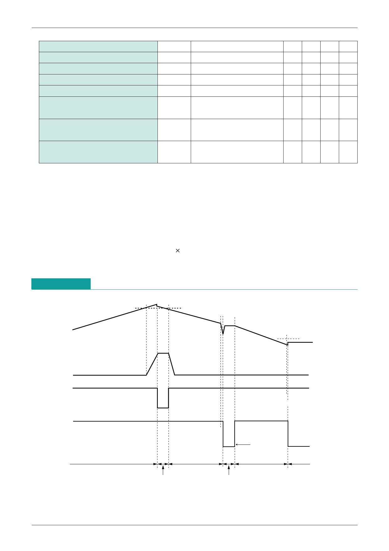
Timing Chart
Overcharge cutoff voltage
Cell voltage
Overcharge expulsion voltage
Overdischarge expulsion voltage
TD
FET gate (charge control)
Overdischarge cutoff voltage
FET gate (discharge control)
removing load
Normal mode
Normal mode
Normal mode
Overcharge mode
Overcurrent
Share Link: 