MM1291 查看數據表(PDF) - Mitsumi
零件编号
产品描述 (功能)
生产厂家
MM1291 Datasheet PDF : 7 Pages
| |||
MITSUMI
Protection of Lithium Ion Batteries (one cell) MM1291
MM1291BFBE
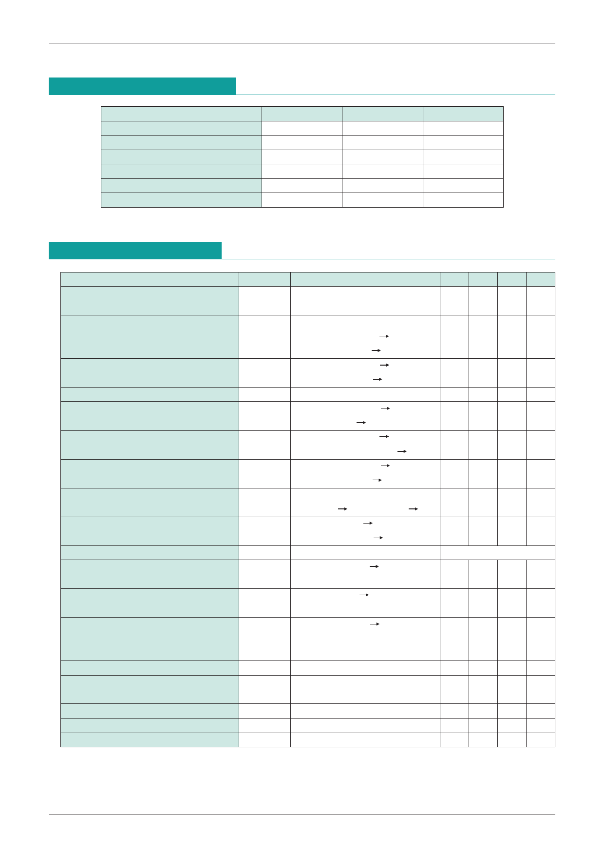
Absolute Maximum Ratings (Ta=25°C)
Item
Symbol
Rating
Units
Storage temperature
TSTG
-40~+125
°C
Operating temperature
TOPR
-20~+70
°C
Power supply voltage
VCC
-0.3~+18
V
VCC-OC pin voltage
VOC
-18~0
V
CS pin voltage
VCS
-0.6~VCC
V
Allowable loss
PD
300
mV
*The CS pin will not cause abnormal operation when connected to protection resistor RCS (=4.7kΩ)
Electrical Characteristics (Unless otherwise specified Ta=25°C, VCC=VIN=3.5V, VCS=0V, Measurement circuit 1, SW1 : a)
Item
Symbol Measurement Conditions Min. Typ. Max. Units
1 (Normal mode) (IS1=ICC+IIN)
ICC1
VCC=VIN=3.5V
10.0 14.0 µA
Consumption current 2 (Overdischarge mode) IOP2
VCC=VIN=1.9V
0.7 1.0 µA
Ta=-20°C~70°C
Overcharge detection voltage
VALM
VCC=VIN=3.9V 4.4V
4.200 4.250 4.300 V
VOC : L H
Overcharge reset voltage
VALML
VCC=VIN=4.4V 3.9V
VOC : H L
3.950 4.050 4.150 V
Overcharge hysteresis voltage
VOCH
VOC-VOCR
150 200 250 mV
Excess discharge detection voltage 1 VS1
VCC=VIN=3.1V 2.0V
VGD : H L VCS=0V
2.50 2.60 2.70 V
Excess discharge detection voltage 2 VS2
VCC=VIN=3.1V 2.0V
VCS=0.05V, VGD : H L
2.30 2.40 2.50 V
Excess discharge reset voltage
VDF
VCC=VIN=2.0V 3.1V
VGD : L H
2.78 2.90 3.02 V
Starting voltage
VCC=VIN=2.75V
VST
-0.3 -0.1
V
VCS : 0V -0.5V, VGD : L H
Overcurrent detection voltage
VCS
VCS=0V 0.12V
VGD : H L
90 100 110 mV
Overcurrent protection release
load release (more than 5 MEG)
Excess discharge detection
non-induction time
tOD
* VCC=VIN=3.0V 2.4V, 1
5.0 10.0 15.0 mS
measurement circuit 2, SW1 : b, SW2 : a
Excessive current detection during
non-induction time
tOC1
* VCS=0V VCS, 1
5.0 10.0 15.0 mS
measurement circuit 2, SW1 : a, SW2 : b
Overcurrent non-induction time
* VCC=VIN=4.0V 4.5V, 1
tALM measurement circuit 2, SW1 : b, SW2 : a 0.5 1.0 1.5 S
CTD=0.082µF
* Operating limit voltage 2
GD pin output voltage H
VOP
VGDH
VCC When VGDL2 > 0.4V
VCC=VIN=3.5V
1.2 V
VCC VCC
V
-0.3 -0.1
GD pin output voltage L1
VGDL1
VCS > 1.0V
0.1 0.3 V
GD pin output voltage L2
VGDL2
VCC=VIN=3.5V, VCS=0.5V
0.2 0.4 V
OC pin output current
IOC
VCC=VIN=4.5V, SW1 : b
-30 uA
*1 Refer to input waveforms.
*2 Operation is unstable below the operating limit voltage.
Share Link: 