LTC1156 查看數據表(PDF) - Linear Technology
零件编号
产品描述 (功能)
生产厂家
LTC1156 Datasheet PDF : 8 Pages
| |||
LTC1156
OPERATIO
A voltage regulator with low standby current provides
continuous bias for the TTL to CMOS converters. The TTL
to CMOS converter output enables the rest of the circuitry.
In this way the power consumption is kept to a minimum
in the standby mode.
Internal Voltage Regulation
The output of the TTL to CMOS converter drives two
regulated supplies which power the low voltage CMOS
logic and analog blocks. The regulator outputs are isolated
from each other so that the noise generated by the charge
pump logic is not coupled into the 100mV reference or the
analog comparator.
Gate Charge Pump
Gate drive for the power MOSFET is produced by an
adaptive charge pump circuit which generates a gate
voltage substantially higher than the power supply volt-
age. The charge pump capacitors are included on chip and
therefore no external components are required to generate
the gate drive.
Drain Current Sense
The LTC1156 is configured to sense the drain current of
the power MOSFET in high side applications. An internal
100mV reference is compared to the drop across a sense
resistor (typically 0.002Ω to 0.1Ω) in series with the drain
lead. If the drop across this resistor exceeds the internal
100mV threshold, the input latch is reset and the gate is
quickly discharged by a large N-channel transistor. A
simple RC network can be added to delay the over-current
protection so that large in-rush current loads such as
lamps or capacitors can be started.
Supply and Ground Pins
The two supply pins (3 and 8) of the LTC1156 must be
connected together at all times and the two ground pins (1
and 6) must be connected together at all times. The two
supply pins should be connected to the “top” of the drain
current sense resistor/s to ensure accurate sensing.
For further applications information, see the LTC1155
Dual High Side Micropower MOSFET Driver data sheet.
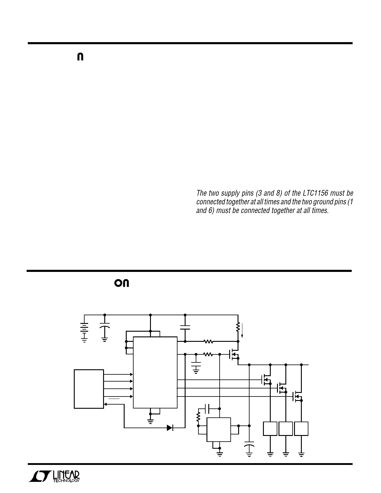
TYPICAL APPLICATI S
4-Cell Extremely Low Voltage Drop Regulator and Three Load
Switches with Short-Circuit Protection and 20µA Standby Current
+
5.2V TO 6V
4-CELL NiCd
BATTERY PACK
+
47µF
DS2 VS VS DS1
DS3
DS4
G1
CONTROL
LOGIC
REG ON/OFF IN1 LTC1156
IN2
G2
IN3
G3
FAULT
IN4
G4
GND GND
0.1µF
100k
**0.03Ω
3.3A MAX
100k
0.1µF
IRLR024
200pF
5V/2A
SWITCHED
2 × Si9956DY
10k
1N4148
* CAPACITOR ESR LESS THAN 0.5Ω
** RCS02 ULTRONIX (303) 242-0810
1
8
3
7 LT1431 4
65
5V 5V 5V
LOAD LOAD LOAD
+
*470µF
1156 TA02
5
Share Link: 