MX809 查看數據表(PDF) - MX-COM Inc
零件编号
产品描述 (功能)
生产厂家
MX809 Datasheet PDF : 22 Pages
| |||
MSK Modem
8
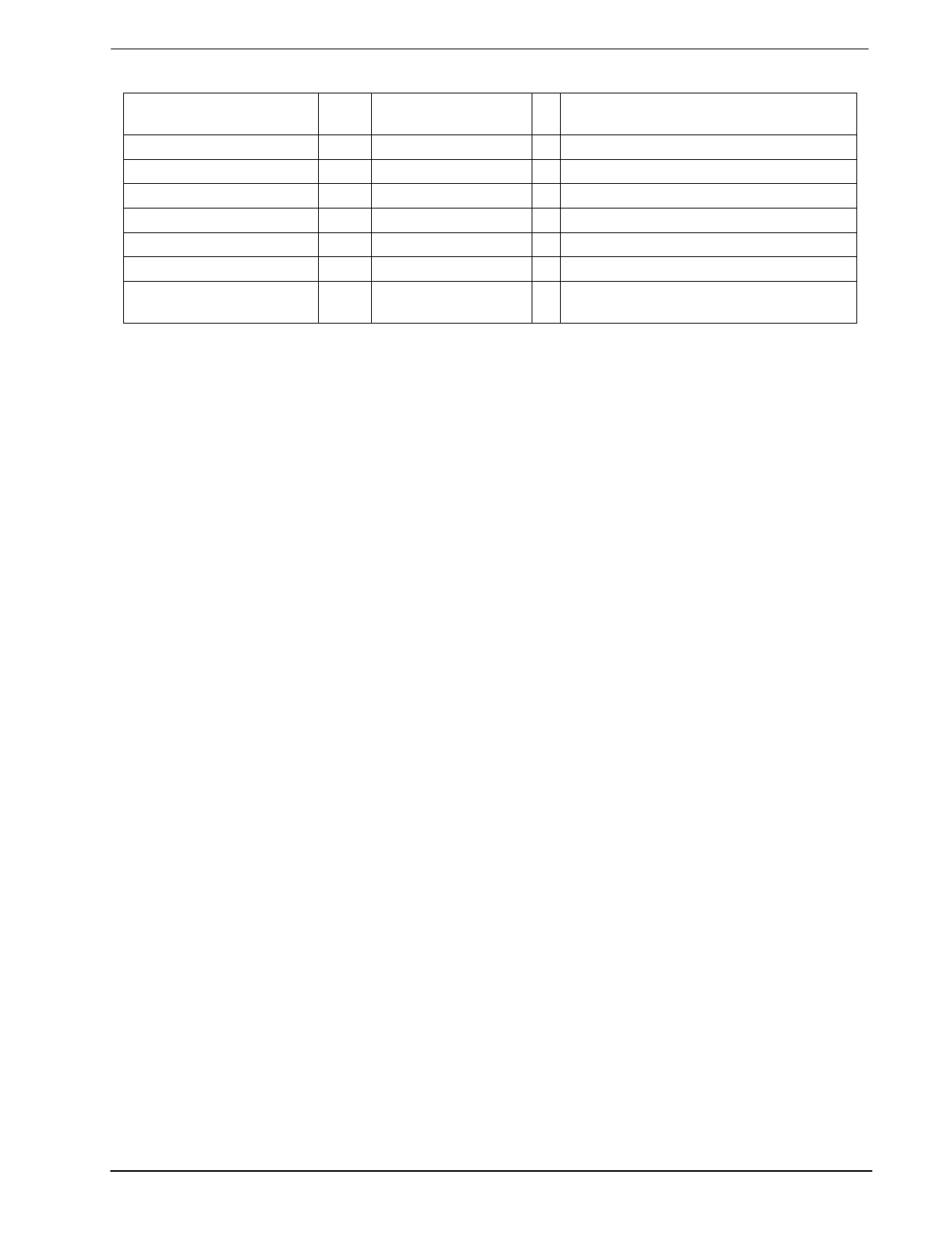
C-BUS allocations for the MX809 are shown in Table 5 and Table 6.
MX809
Command Assignment
General Reset
Write to Control Register
Read Status Register
Read RX Data Buffer
Write to TX Data Buffer
Write to SYNC Program
Address/Command
Binary
Command Data
HEX
MSB LSB
01
00000001
Control Register bits set to logic “0”
48
01001000
+ 1 byte instruction to Control Register
49
01001001
+ 1 byte reply from Status Register
4A
01001010
+ 1 byte of data from RX Data Buffer
4B
01001011
+ 1 byte of data to TX Data Buffer
4C
01001100
+ 2 bytes of SYNC Word to SYNC
Program Register
Table 6: Modem No. 2 C-BUS Address/Commands – (Address Select input at a logic “1”)
5.2 Address Select
This input allows 2 MSK Modems on the same BUS, using the correct addressing.
When operating in a system using 2 MSK Modems, one MSK Modem is designated No. 1 and requires its
Address Select input to be held at a logic “0”. The second Modem (No. 2) requires its Address select input to
be held at logic “1”.
All C-BUS transactions with Modem 1 will use Address/Command allocations 40H to 44H (Table 5) and
transactions with Modem 2 will use 48H to 4CH (Table 6).
For explanation purposes, further descriptions of MX809 MSK Modem internal register functions will deal
primarily with MSK Modem No. 1 (Address Select at logic “0”).
1998 MX-COM, Inc.
www.mxcom.com Tel: 800 638 5577 336 744 5050 Fax: 336 744 5054
Doc. # 20480036.004
4800 Bethania Station Road, Winston-Salem, NC 27105-1201 USA
All trademarks and service marks are held by their respective companies.
Share Link: 