ML2502 查看數據表(PDF) - Oki Electric Industry
零件编号
产品描述 (功能)
生产厂家
ML2502 Datasheet PDF : 20 Pages
| |||
OKI
n PIN DESCRIPTION
ML2502
PIN
REC1
REC2
PLAY1
PLAY2
ERASE
SAM1
SAM2
I/O
Description
Input start-recording signal for Phrase 1 to this pin.
I
"H" level input to this pin initiates recording to Phrase 1 memory area. Recording goes on
while this pin being held "H". In single-phrase mode, the pin is connected to the REC2 pin.
The REC1 pin is internally pulled down.
Input start-recording signal for Phrase 2 to this pin.
I
"H" level input to this pin initiates recording to Phrase 2 memory area. Recording goes on
while this pin being held "H". In single phrase mode, the pin is connected to the REC1 pin.
The REC2 pin is internally pulled down.
Input start-playback signal for Phrase 1 to this pin.
I
A "H" pulse input to this pin initiates playback of Phrase 1. Re-inputting a "H" pulse during
playback causes to stop playback. In single phrase mode, the pin is connected to the
PLAY2 pin. The pin is internally pulled down.
Input start-playback signal for Phrase 2 to this pin.
I
A "H" pulse input to this pin initiates playback of Phrase 2. Re-inputting a "H" pulse during
playback causes to stop playback. In single phrase mode, the pin is connected to the
PLAY1 pin. The pin is internally pulled down.
Erase-enable signal input pin, used together with the REC1 and/or REC2.
I
Input "H" level to the REC1/REC2 pin with this pin being held "H" to erase respective
phrase.
The pin is internally pulled down.
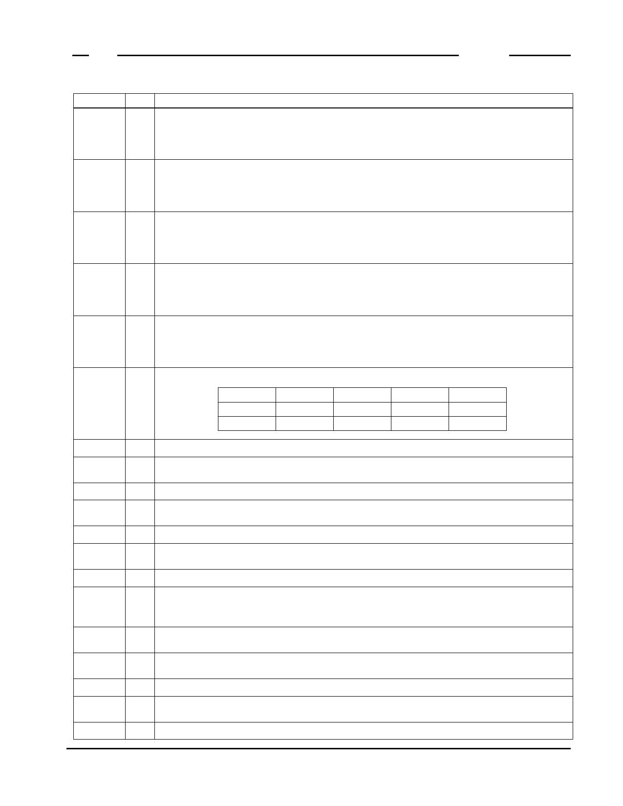
Pins used to select a sampling frequency.
I
SAM1
L
L
H
H
SAM1
L
H
L
H
Fs
4.0kHz
5.3kHz
6.4kHz Unused
MON O Output "H" level during record or playback operation.
ROSC
I
Insert a 30kΩ resistor between this pin and the DGND pin. The resistor determines the
oscillation frequency for the internal oscillation circuit.
MIN
I Input to the Microphone amplifier.
MOUT
O
Output from the Microphone amplifier. Voltage amplitude is automatically controlled to an
appropriate output level by the internal AGC circuit.
LIN
I Input to the Line amplifier. Connected to inverted input for the internal Op. amplifier.
LOUT
O
Output from the Line amplifier. Connected to the output pin from the internal Op. amplifier.
Connecting resistors to the LIN and LOUT pins configures an inverted amplifier.
AOUT O Output analog signal for playback.
SPIN
Input to the speaker driver. The resistor's value inserted between the AOUT and SPIN pin
I determines voltage amplitude of the speaker driver. Select an appropriate value
depending on types of speaker in use.
SPOUT+
SPOUT-
O
Output from the speaker driver. Connect a speaker in-between these pins.
Output two phase-inverted analog signals for playback from the speaker driver.
DVDD
−
Digital power supply pin. Insert a 0.1µF or larger bypass capacitor between this pin and
the DGND pin.
DGND
AVDD
− Digital ground pin.
−
Analog power supply pin. Insert a 0.1µF or larger bypass capacitor between this pin and
the AGND pin.
AGND − Analog ground pin.
ML2502 Data Sheet (Revision 8.0)
3
Share Link: 