NT128S64VH4A0GM0-8B 查看數據表(PDF) - Nanya Technology
零件编号
产品描述 (功能)
生产厂家
NT128S64VH4A0GM0-8B
Nanya Technology

NT128S64VH4A0GM0-8B Datasheet PDF : 12 Pages
| |||
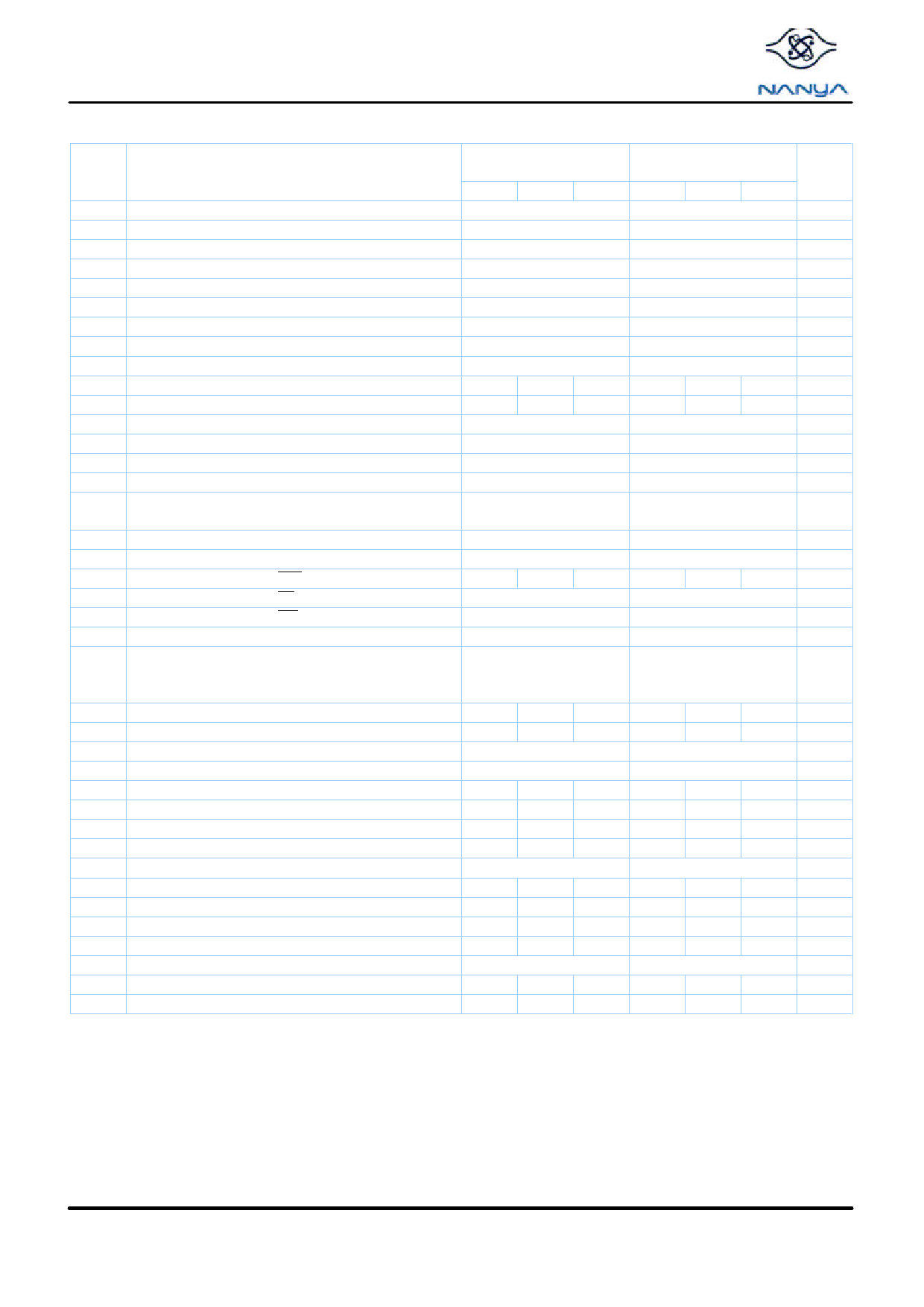
NT128S64VH4A0GM
128MB : 16M x 64
SDRAM SODIMM
Serial Presence Detect -- Part 1 of 2
16Mx64 SDRAM SODIMM based on 16Mx16, 4Banks, 8K Refresh, 3.3V SDRAMs with SPD
Byte
Description
SPD Entry Value
Serial PD Data Entry
(Hexadecimal)
-7K
-75B
-8B
-7K
-75
-8B
0 Number of Serial PD Bytes Written during Production
128
80
1 Total Number of Bytes in Serial PD device
256
08
2 Fundamental Memory Type
SDRAM
04
3 Number of Row Addresses on Assembly
13
0D
4 Number of Column Addresses on Assembly
9
09
5 Number of DIMM Bank
1
01
6 Data Width of Assembly
X64
40
7 Data Width of Assembly (cont’)
X64
00
8 Voltage Interface Level of this Assembly
LVTTL
01
9 SDRAM Device Cycle Time at CL=3
7ns 7.5ns 8ns
70
75
80
10 SDRAM Device Access Time from Clock at CL=3
5.4ns 5.4ns 6ns
54
54
60
11 DIMM Configuration Type
Non-Parity
00
12 Refresh Rate/Type
7.8µs / SR
82
13 Primary SDRAM Width
X16
10
14 Error Checking SDRAM Device Width
N/A
00
SDRAM Device Attributes :
15
Minimum Clock Delay, Random Column Access
1 Clock
01
16 SDRAM Device Attributes: Burst Length Supported
1,2,4,8
0F
17 SDRAM Device Attributes: Number of Device Banks
4
04
18 SDRAM Device Attributes: CAS Latency
2, 3
2, 3
2, 3
06
06
06
19 SDRAM Device Attributes: CS Latency
0
01
20 SDRAM Device Attributes: WE Latency
0
01
21 SDRAM Module Attributes
Unbuffered
00
Wr-1/Rd Burst, Precharge All,
22 SDRAM Device Attributes: General
Auto-Precharge, VDD +/-
0E
10%
23 Minimum Clock Cycle at CL=2
7.5ns 10ns 10ns
75
A0
A0
24 Maximum Data Access Time from Clock at CL=2
5.4ns 6ns
6ns
54
60
60
25 Minimum Clock Cycle Time at CL=1
N/A
00
26 Maximum Data Access Time from Clock at CL=1
N/A
00
27 Minimum Row Precharge Time (tRP)
15ns 20ns 20ns
0F
14
14
28 Minimum Row Active to Row Active delay (tRRD)
15ns 15ns 20ns
0F
0F
14
29 Minimum RAS to CAS delay (tRCD)
15ns 20ns 20ns
0F
14
14
30 Minimum RAS Pulse Width (tRAS)
45ns 45ns 50ns
2D
2D
32
31 Module Bank Density
128MB
20
32 Address and Command Setup Time Before Clock
1.5ns 1.5ns 2ns
15
15
20
33 Address and Command Hold Time After Clock
0.8ns 0.8ns 1ns
08
08
10
34 Data Input Setup Time Before Clock
1.5ns 1.5ns 2ns
15
15
20
35 Data Input Hold Time After Clock
0.8ns 0.8ns 1ns
08
08
10
36-61 Reserved
Undefined
00
62 SPD Revision
1.2
1.2
1.2
12
12
12
63 Checksum for bytes 0 - 62
F3
39
80
Note
PRELIMINARY 08 /2001
10
© NANYA TECHNOLOGY CORP.
NANYA TECHNOLOGY CORP. reserves the right to change Products and Specifications without notice.
Share Link: