ICS9110-01CS14 查看數據表(PDF) - Integrated Circuit Systems
零件编号
产品描述 (功能)
生产厂家
ICS9110-01CS14 Datasheet PDF : 10 Pages
| |||
AV9110
Serial Programming
The AV9110 is programmed to generate clock frequencies by
entering data through the shift register. Figure 1 displays the
proper timing sequence. On the negative going edge of CE#,
the shift register is enabled and the data at the DATA pin is
loaded into the shift register on the rising edge of the SCLK.
Bit D0 is loaded first, followed by D1, D2, etc. This data
consists of the 24 bits shown in the Shift Register Bit
Assignment in Table 1, and therefore takes 24 clock cycles to
load. An internal counter then disables the input and transfers
the data to internal latches on the rising edge of the 24th
cycle of the SCLK. Any data entered after the 24th cycle is
ignored until CE# must remain low for a minimum of 24 SLCK
clock cycles. If CE# is taken high before 24 clock cycles have
elapsed, the data is ignored (no frequency change occurs)
and the counter is reset. Tables 1 and 2 display the bit location
for generating the output clock frequency and the output
divider circuitry, respectively.
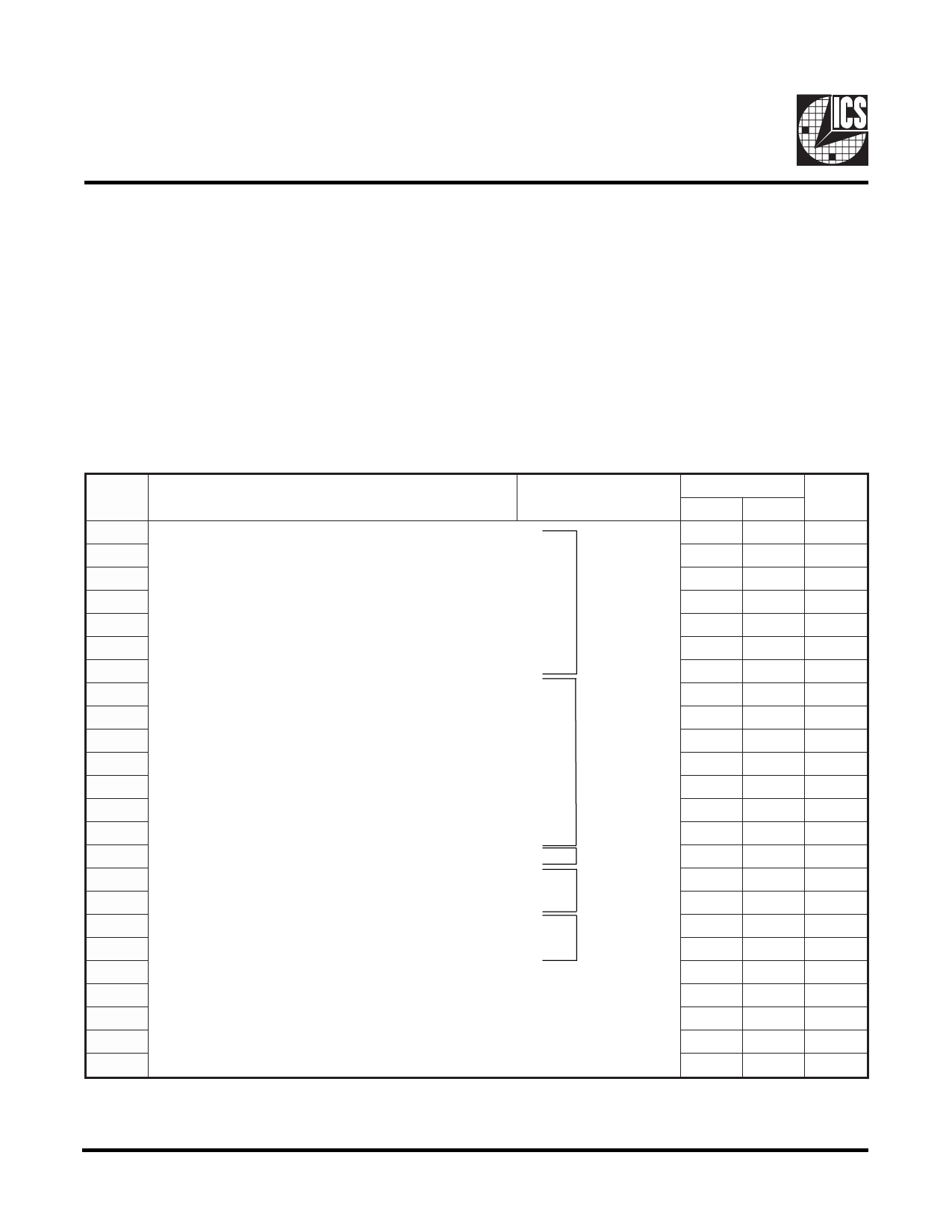
BIT
ASSIGNMENT
0 VCO frequency divider (LSB)
1 VCO frequency divider
2 VCO frequency divider
3 VCO frequency divider
4 VCO frequency divider
5 VCO frequency divider
6 VCO frequency divider (MSB)
7 Reference frequency divider (LSB)
8 Reference frequency divider
9 Reference frequency divider
10 Reference frequency divider
11 Reference frequency divider
12 Reference frequency divider
13 Reference frequency divider (MSB)
14 VCO pre-scale divide (0=divide by 1, 1=divide by 8
15 CLK/X output divide COD0 (see Table 2)
16 CLK/X output divide COD1 (see Table 2)
17 VCO output divide VOD0 (see Table 3)
18 VCO output divide VOD1 (see Table 3)
19 Outplut enable CLK (0=tristate)
20 Output enable CLK/X (0=tristate)
21 Reserved. Should be programmmed high (1)
22 Reference clock select on CLK (1 = reference frequency)
23 Reserved. Should be programmed high (1)
EQUATION
VARIABLE
N
Integer
M
Integer
V
X
R
DEFAULT
BIT
-01
-02
1
1
0
1
1
1
1
1
2
1
1
3
1
1
4
1
1
5
1
1
6
0
0
7
1
1
8
0
0
9
0
0
10
1
1
11
0
0
12
0
0
13
0
0
14
0
1
15
1
0
16
0
0
17
1
1
18
1
1
19
1
1
20
1
1
21
0
0
22
1
1
23
4
Share Link: 