SN74LS164 查看數據表(PDF) - Motorola => Freescale
零件编号
产品描述 (功能)
生产厂家
SN74LS164 Datasheet PDF : 4 Pages
| |||
SN54 / 74LS164
A
1
2
B
8 CP
DQ
CD
DQ
CD
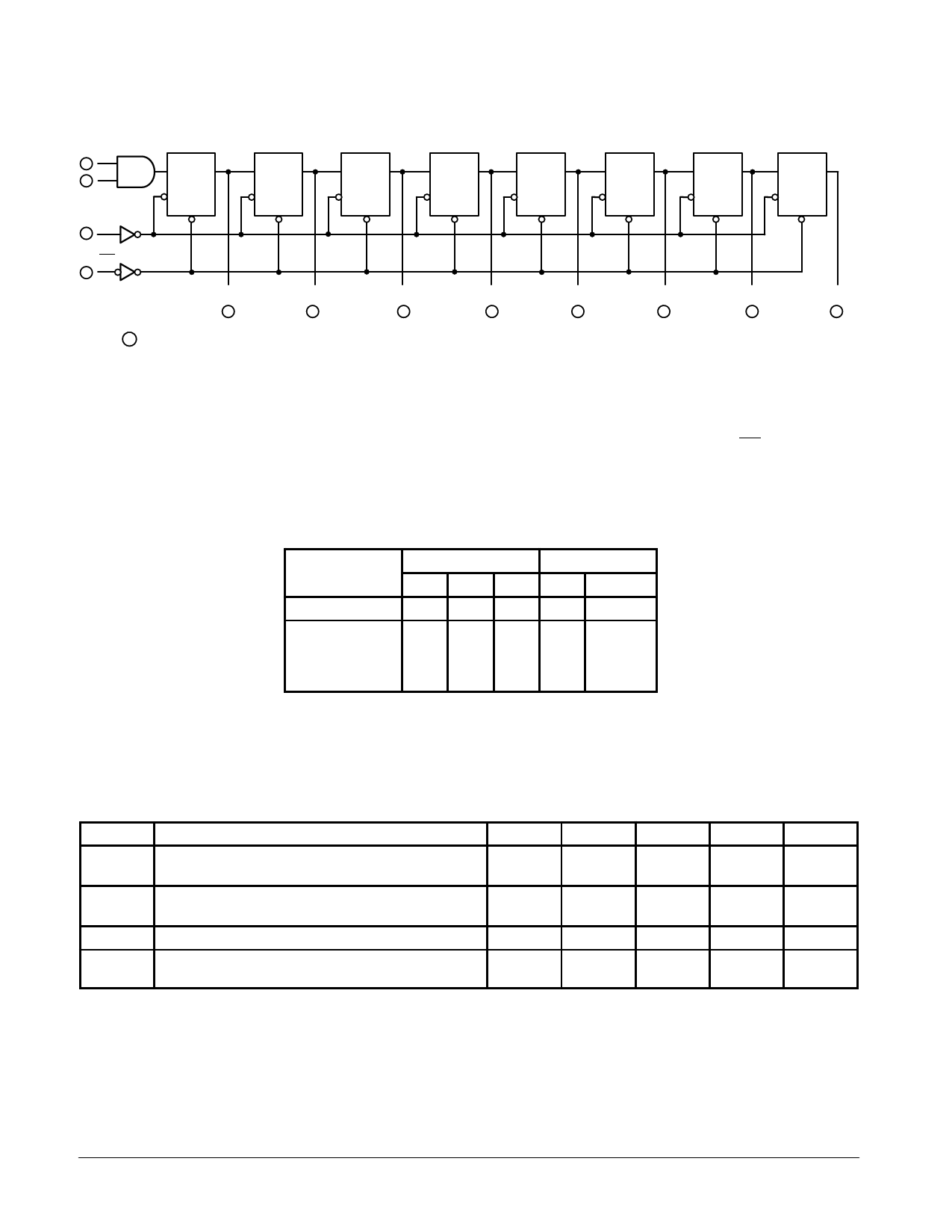
LOGIC DIAGRAM
DQ
CD
DQ
CD
DQ
CD
DQ
CD
DQ
CD
DQ
CD
MR
9
Q0
Q1
Q2
Q3
Q4
Q5
Q6
Q7
VCC = PIN 14
3
4
5
6
10
11
12
13
GND = PIN 7
= PIN NUMBERS
FUNCTIONAL DESCRIPTION
The LS164 is an edge-triggered 8-bit shift register with seri-
al data entry and an output from each of the eight stages. Data
is entered serially through one of two inputs (A or B); either of
these inputs can be used as an active HIGH Enable for data
entry through the other input. An unused input must be tied
HIGH, or both inputs connected together.
Each LOW-to-HIGH transition on the Clock (CP) input shifts
data one place to the right and enters into Q0 the logical AND
of the two data inputs (A•B) that existed before the rising clock
edge. A LOW level on the Master Reset (MR) input overrides
all other inputs and clears the register asynchronously, forcing
all Q outputs LOW.
MODE SELECT — TRUTH TABLE
OPERATING
MODE
Reset (Clear)
INPUTS
MR A
B
L
X
X
OUTPUTS
Q0
Q1–Q7
L
L–L
Shift
H
I
I
L
q0 – q6
H
I
h
L
q0 – q6
H
h
I
L
q0 – q6
H
h
h
H
q0 – q6
L (l) = LOW Voltage Levels
H (h) = HIGH Voltage Levels
X = Don’t Care
qn = Lower case letters indicate the state of the referenced input or output one
qn = set-up time prior to the LOW to HIGH clock transition.
GUARANTEED OPERATING RANGES
Symbol
Parameter
VCC
Supply Voltage
TA
Operating Ambient Temperature Range
IOH
Output Current — High
IOL
Output Current — Low
Min
Typ
54
4.5
5.0
74
4.75
5.0
54
– 55
25
74
0
25
54, 74
54
74
Max
5.5
5.25
125
70
– 0.4
4.0
8.0
Unit
V
°C
mA
mA
FAST AND LS TTL DATA
5-2
Share Link: 