NT128S64V88C0G-75B 查看數據表(PDF) - Nanya Technology
零件编号
产品描述 (功能)
生产厂家
NT128S64V88C0G-75B Datasheet PDF : 12 Pages
| |||
NT128S64V88C0G
128MB : 16M x 64
Unbuffered SDRAM Module
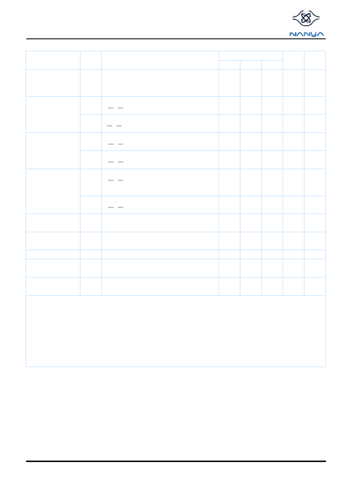
Operating, Standby, and Refresh Currents (T A =0 to 70 °C , V DD =3.3 ± 0.3V)
Parameter
Symbol
Test condition
Operating current
ICC1
Precharge
standby current
in power-down mode
ICC2P
ICC2PS
Precharge
standby current in non
power-down mode
ICC2N
ICC2NS
No Operating current
( Active state : 4 bank)
ICC3P
ICC3N
Operating current
( Burst mode )
ICC4
Auto(CBR)
ICC5
refresh current
1 bank operation , tRC = tRC(mim), tCK = min
Active-Precharge Command cycling
without burst operation
CKE0 <= VIL (max), tCK = min,
S0 , S2 = VIH (min)
CKE0 <= VIL (max), tCK =oo,
S0 , S2 = VIH (min)
CKE0 >= VIH (min), tCK = min
S0 , S2 = VIH (min)
CKE0 >= VIH (min), tCK =oo,
S0 , S2 = VIH (min)
CKE0 <= VIL (max), tCK =min.
S0 , S2 = VIH (min)
(Power Down Mode)
CKE0 >= VIH (min), tCK =min
S0 , S2 = VIH (min)
tCK =min , Read/ Write command cycling,
Multiple banks active, gapless data, BL=4
tCK =min, CBR command cycling
Speed
Unit Note
- 7K - 75B - 8B
720
680
640
mA
1, 2
16
16
16
mA
16
16
16
mA
400
360
280
mA
3
72
72
72
mA
4
72
72
72
mA
5
480
400
320
mA
3
1080 960
810
mA
2, 6
1520 1520 1360
mA
Self refresh current
Serial PD Device
Standby Current
ICC6
ISB
CKE0 <= 0.2V
VIN = GND or VDD
16
16
16
mA
30
30
30
µA
7
Serial PD Device Active
Power Supply Current
ICCA
SCL Clock Frequency=100 MHz
1
1
1
µA
8
1. These parameters depend on the cycle rate and are measured with the cycle determined by the minimum value of t CK and t RC . Input
signals are changed up to three times during t RC (min).
2. The specified values are obtained with the output open.
3. Input signals are changed once during three clock cycles.
4. Input signals are stable.
5. Active standby current will be higher if Clock Suspend is entered during a Burst Read cycle (add 1mA per DQ).
6. Input signals are changed once during t ck(min) .
7. VDD =3.3V
8. Input pulse levels VDD x 0.1 to VDD x 0.9, input rise and fall times 10ns, input and output timing levels VDD x 0.5, output load 1 TTL gate and
CL=100pF.
REV 1.0 07 / 2001
6
© NANYA TECHNOLOGY CORP.
NANYA TECHNOLOGY CORP. reserves the right to change Products and Specifications without notice.
Share Link: 