M38072MA-XXXFS 查看數據表(PDF) - MITSUBISHI ELECTRIC
零件编号
产品描述 (功能)
生产厂家
M38072MA-XXXFS Datasheet PDF : 74 Pages
| |||
MITSUBISHI MICROCOMPUTERS
3807 Group
SINGLE-CHIP 8-BIT CMOS MICROCOMPUTER
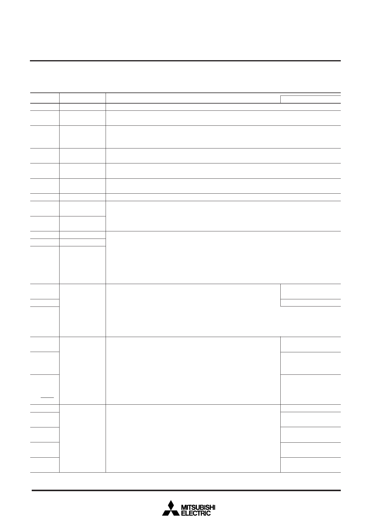
PIN DESCRIPTION
Table. 1. Pin description (1)
Pin
Name
Function
Function except a port function
VCC, VSS Power source
• Apply voltage of 2.7–5.5 V to VCC, and 0 V to VSS.
CMPVCC Analog comparator • Power source input pin for an analog comparator
power source
CNVSS
CNVSS
• This pin controls the operation mode of the chip.
• Normally connected to VSS.
• If this pin is connected to VCC, the internal ROM is inhibited and external memory is accessed.
ADVREF Analog reference • Reference voltage input pin for A-D converter.
voltage
AVSS
Analog power
• Analog power source input pin for A-D and D-A converter and an analog comparator
source
• Connect to VSS.
CMPOUT Analog comparator • Output pin for an analog comparator
______
RESET
output
Reset input
• Reset input pin for active “L”
XIN
Clock input
• Input and output signals for the internal clock generating circuit.
• Connect a ceramic resonator or quartz-crystal oscillator between the XIN and XOUT pins to set the oscillation frequency.
XOUT
Clock output
• If an external clock is used, connect the clock source to the XIN pin and leave the XOUT pin open.
• The clock is used as the oscillating source of system clock.
P00–P07 I/O port P0
• 8-bit CMOS I/O port
P10–P17 I/O port P1
• I/O direction register allows each pin to be individually programmed as either input or output.
P20–P27 I/O port P2
• At reset this port is set to input mode.
• In modes other than single-chip, these pins are used as address, data bus I/O pins.
• CMOS compatible input level
• CMOS 3-state output structure
• Port P2 can be switched CMOS or TTL input level.
P30/RTP6, I/O port P3
• 8-bit CMOS I/O port
• Real time port function
P31/RTP7
• I/O direction register allows each pin to be individually programmed as either input or output. pins
P34/CKOUT,
• At reset this port is set to input mode.
• Clock output function pin
P32, P33,
• In modes other than single-chip, these pins are used as control bus I/O pins.
P35–P37
• CMOS compatible input level
• CMOS 3-state output structure
• Port P32 can be switched CMOS or TTL input level.
P40/XCOUT, I/O port P4
• 8-bit CMOS I/O port with the same function as port P0
• Sub-clock generating I/O
P41/XCIN
• CMOS compatible input level
pins(connect a resonator)
P42/INT0,
• CMOS 3-state output structures
• Interrupt input pins
P43/INT1
• Timer X, Timer Y function pins
(INT0, INT1)
P44/RXD,
• Serial I/O1 function pins
P45/TXD,
P46/SCLK1,
P47/SRDY1
P50/TOUT I/O port P5
• 8-bit CMOS I/O port with the same function as port P0
• Timer 2 output pin
P51/SCMP2/
• CMOS compatible input level
• Interrupt input pin
INT2
• CMOS 3-state output structure
• Serial I/O2 function pin
P52/INT3,
• Interrupt input pin
P53/INT4
• Real time port function pin(INT4)
P54/CNTR0,
• Timer X, Timer Y function pins
P55/CNTR1
P56/DA1,
• D-A conversion output
P57/DA2
pins
3
Share Link: 