LC7233N-8818 查看數據表(PDF) - SANYO -> Panasonic
零件编号
产品描述 (功能)
生产厂家
LC7233N-8818 Datasheet PDF : 36 Pages
| |||
LC7233N-8818
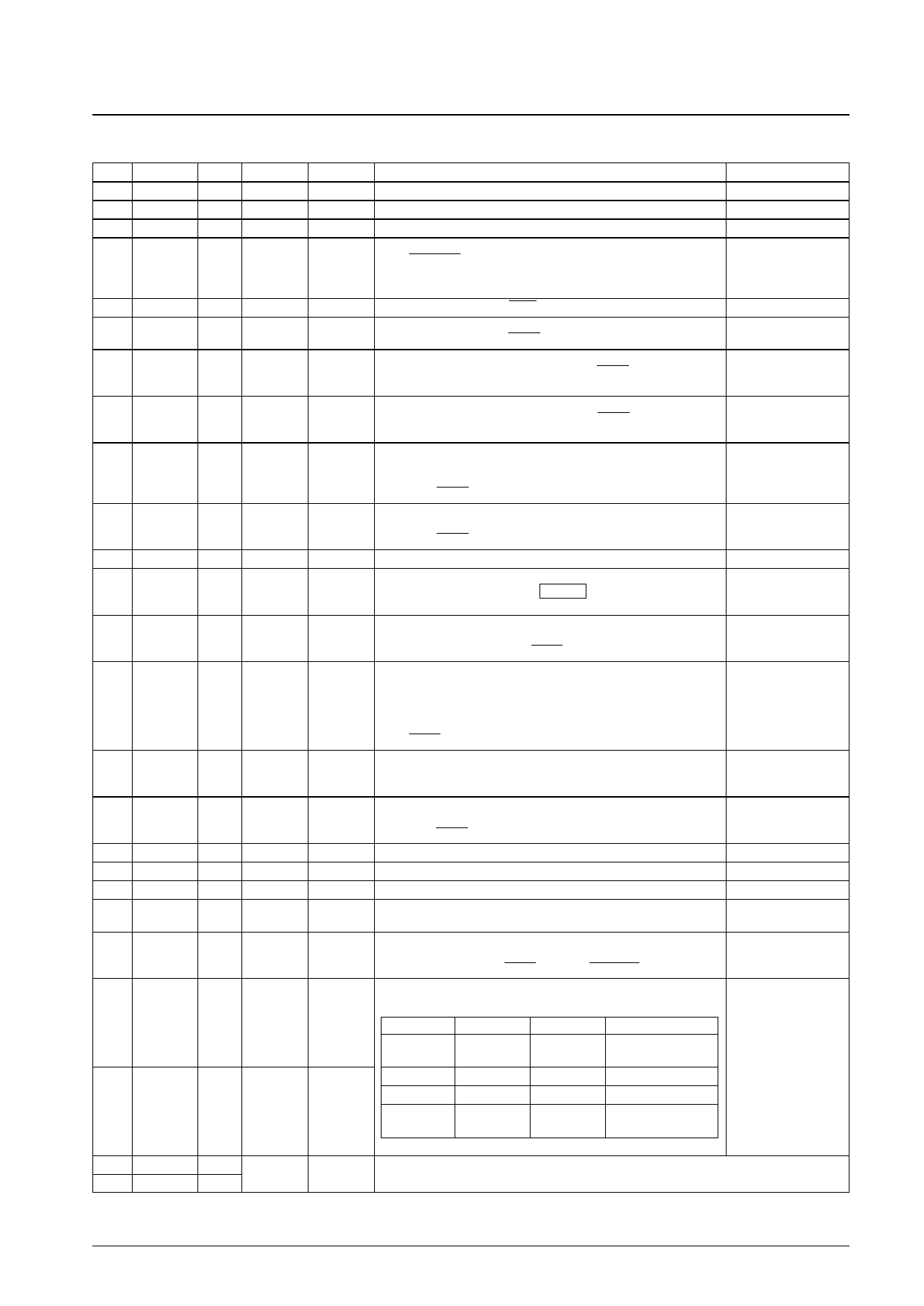
Continued from preceding page.
Pin
Name
27
S23
28
S22
29
S21
30
S20
31
S19
32
S18
33
S17
34
S16
35
S15
36
S14
37
S13
38
S12
39
S11
40
S10
41
S9
42
S8
43
S7
44
S6
45
S5
46
S4
47
S3
48
S2
49
S1
50
COM2
51
COM1
I/O Allocation
O
T5
O
T6
O
T7
O LEDFLSH
O
DKOUT
O
MUTE
O
APS
O
MTL
O
NR2
O
NR1
O
CDOUT
O
POWER
O
LOC
O
MO/ST
O
IFCNT
O
LOUD
O
DI
O
CL
O
CE
O
FMLOW
O
MODE
O
BAND2
O
BAND1
O
—
O
Active
H
H
H
H
H
H
H
H
H
H
H
H
H
H
H
H
H
H/L
H
H
H/L
H/L
H/L
—
Function
Diode scan out
Diode scan out
Diode scan out
Outputs a high level for 0.25 second and a low level for 0.75 second
when PANEL IN goes high. However, the LC7233N-8818 only
performs this operation when the diode matrix LED FLASH setting is
0.
Outputs a high level when DKIN goes low.
Inverted by the mute key. When high, the volume level display flashes
at a 1 Hz rate. Valid when HOLD is high and main power is on.
In tape mode, outputs a high level when the APS display is lit, and a
low level when that display is off. Valid when HOLD is high and main
power is on.
In tape mode, outputs a high level when the MTL display is lit, and a
low level when that display is off. Valid when HOLD is high and main
power is on.
In tape mode when the diode matrix NR setting is 1 (i.e., when DNR-
C is selected), outputs a high level when the DNR display and the C
in the preset CH digit are lit, and a low level when that display is off.
Valid when HOLD is high and main power is on.
In tape mode, outputs a high level when the DNR display and the B in
the preset CH digit are lit, and a low level when that display is off.
Valid when HOLD is high and main power is on.
CD source switch (See the CDIN pin description.)
Outputs a high level when the power is on (when the diode matrix
POWER SW setting is 1 and the POWER key is on). Outputs low
when power is off.
In radio mode when the LOC display is lit, outputs a high level only
during seek or scan when a seek or scan is started. Outputs low
when display is off. Valid when HOLD is high and main power is on.
In radio mode during FM reception (including VF and radio monitor),
outputs a low level when the ST display is lit, and a high level when
that display is off. However, note that this output is enabled for the US
and Japanese MW band when the diode matrix AM ST SEL setting is
0. Outputs a low level in other modes, i.e., tape or CD mode, and
when HOLD is low (clock enabled).
This signal switches the IF counter buffer on and off. Outputs a high
level only when there is an SD during auto search, otherwise outputs
a low level.
Outputs a high level when the LOUD display is lit, and a low level
when that display is off.
Valid when HOLD is high and main power is on.
Connected to the LC7538JMD DATA pin.
Connected to the LC7538JMD CLOCK pin.
Connected to the LC7538JMD CE pin.
Outputs a high level when the FM band is from 64.0 to 74.0 MHz, and
a low level when the FM band is from 87.5 to 108.0 MHz.
Outputs a high level in radio mode, including when DK is on, and
outputs a low level in tape and CD modes.
Outputs a low level when HOLD is low and PANEL IN is high.
These signals change as shown in the table below when the band
key is pressed.
Handling when unused
Open
Open
Open
Open
Open
Open
Open
Open
Open
Open
Open
Open
Open
Open
Open
Open
Open
Open
Open
Open
Open
BAND
BAND1
MW
0
LW
0
FM
1
VF
1
Note: 0 = Low, 1 = High
BAND2
0
1
0
1
Note
Including tape and
CD modes
Must be used.
Including times when
DK is on
These pins are left open in normal operation.
Continued on next page.
No. 4743-8/36
Share Link: 