28F016S3 查看數據表(PDF) - Intel
零件编号
产品描述 (功能)
生产厂家
28F016S3 Datasheet PDF : 41 Pages
| |||
28F004S3/28F008S3/28F016S3
E
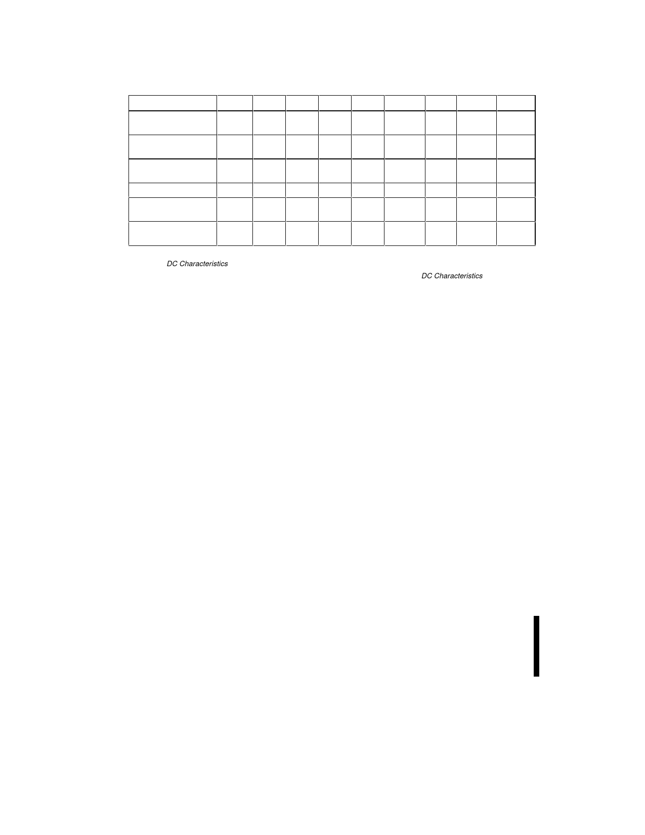
Table 2. Bus Operations
Mode
Notes RP# CE# OE# WE# Address VPP DQ0–7 RY/BY#
Read
1,2,3 VIH or VIL
VIL
VIH
X
VHH
X
DOUT
X
Output Disable
3
VIH or VIL
VIH
VIH
X
VHH
X High Z
X
Standby
3
VIH or VIH
X
X
X
X High Z
X
VHH
Deep Power-Down
4
VIL
X
X
X
X
X
High Z
VOH
Read Identifier Codes
VIH or VIL
VIL
VIH
See
X
Note 5
VOH
VHH
Figure 5
Write
3,6,7 VIH or VIL
VIH
VIL
X
X
DIN
X
VHH
NOTES:
1. Refer to DC Characteristics. When VPP ≤ VPPLK, memory contents can be read, but not altered.
2. X can be VIL or VIH for control and address input pins and VPPLK or VPPH1/2 for VPP. See DC Characteristics for VPPLK and
VPPH1/2 voltages.
3. RY/BY# is VOL when the WSM is executing internal block erase, program, or lock-bit configuration algorithms. It is VOH
when the WSM is not busy, in block erase suspend, program suspend, or deep power-down mode.
4. RP# at GND ± 0.2 V ensures the lowest deep power-down current.
5. See Section 4.2 for read identifier code data.
6. Command writes involving block erase, program, or lock-bit configuration are reliably executed when VPP = VPPH1/2 and
VCC = VCC2 (see Section 6.2 for operating conditions).
7. Refer to Table 3 for valid DIN during a write operation.
14
PRELIMINARY
Share Link: 