LTC1623CMS8 查看數據表(PDF) - Linear Technology
零件编号
产品描述 (功能)
生产厂家
LTC1623CMS8 Datasheet PDF : 12 Pages
| |||
LTC1623
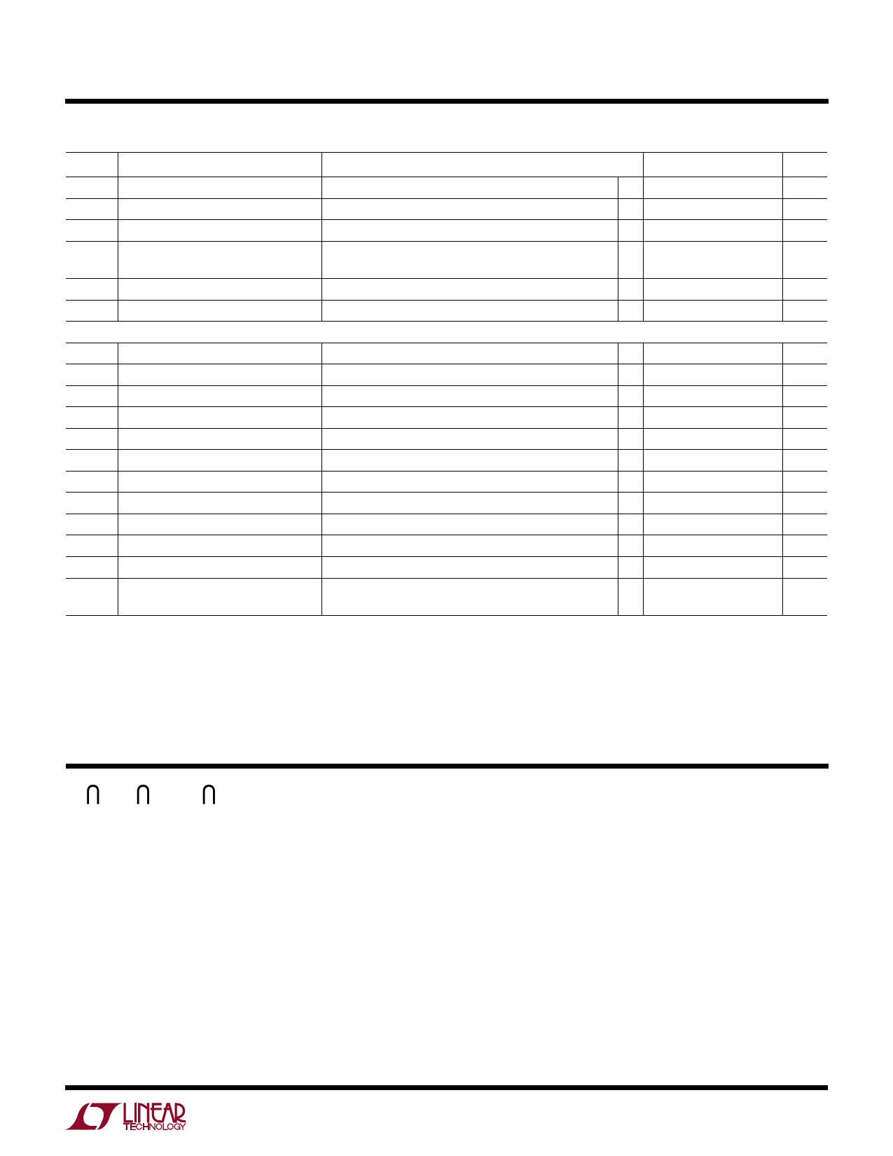
ELECTRICAL CHARACTERISTICS TA = 25°C, VCC = 5V unless otherwise specified. CGA = 1000pF, CGB = 1000pF
SYMBOL PARAMETER
CONDITIONS
MIN TYP MAX UNITS
VIL
AD0 and AD1 Input Low Voltage
VIH
AD0 and AD1 Input High Voltage
VOL
Data Output Low Voltage
CIN
Input Capacitance
(DATA, CLK, AD0, AD1)
VCC = 2.7V to 5.5V
VCC = 2.7V to 5.5V
VCC = 2.7 to 5.5V, IPULLUP = 350µA
q
0.2
V
q VCC – 0.2
V
q
0.22 0.4
V
5
pF
IIN
Input Leakage Current (DATA, CLK)
Input Leakage Current(AD0, AD1)
SMBus Related Specs (Note 6)
±1
µA
±250
nA
fSMB
tSUSTA
tBUF
tHDSTA
tSUSTP
tHDDAT
tSUDAT
tLOW
tHIGH
tf
tr
IPULLUP
SMBus Operating Frequency
Start Condition Setup Time
Bus Free Time Between Stop and Start
Start Condition Hold Time
Stop Condition Setup Time
Data Hold Time
Data Setup Time
Clock Low Period
Clock High Period
Clock /Data Fall Time
Clock/Data Rise Time
Current Through External Pull-Up
Resistor on DATA Pin
(Data Pull-Down Current Capacity)
VCC = 2.7V to 5.5V
10
100
kHz
4.7
µs
4.7
µs
4.0
µs
4.0
µs
300
ns
250
ns
4.7
µs
4.0
50
µs
300
ns
1000
ns
100
350
µA
The q denotes the specifications which apply over the full operating
temperature range.
Note 1: Approximately 3% hysteresis is provided to ensure stable
operation and eliminate false triggering by minor VCC glitches.
Note 2: Measured from VCC > VUVLO to SMBus ready for data input.
Note 3: The oscillator frequency is not tested directly but is inferred from
turn-on time.
Note 4: ON is enabled upon receiving the Stop condition from the SMBus
master.
Note 5: OFF is enabled upon receiving the Stop condition from the SMBus
master.
Note 6: SMBus timing specs are guaranteed but not tested.
PIN FUNCTIONS
DATA: (Pin 1) Open-Drain Connected Serial Data Inter-
face. Must be pulled high to VCC with external resistor. The
pull-up current must be limited to 350µA.
CLK: (Pin 2) Serial Clock Interface. Must be pulled high to
VCC with external resistor. The pull-up current must be
limited to 350µA.
AD0: (Pin 3) Lower Three-State Programmable Address
Pin. Must be connected directly to VCC, GND, or VCC/2
(using two resistors ≤ 1M). Do not float this pin.
GND: (Pin 4) Ground.
AD1: (Pin 5) Higher Three-State Programmable Address
Pin. Must be connected directly to VCC, GND, or VCC/2
(using two resistors ≤ 1M). Do not float this pin.
GB: (Pin 6) Gate Drive to External High-Side Switch. Fully
enhanced by internal charge pump. Controlled by 2nd
LSB of command byte.
GA: (Pin 7) Gate Drive to External High-Side Switch. Fully
enhanced by internal charge pump. Controlled by LSB of
command byte.
VCC: (Pin 8) Input Supply Voltage. Range from 2.7V to
5.5V.
3
Share Link: 