VSC6501RC 查看數據表(PDF) - Vitesse Semiconductor
零件编号
产品描述 (功能)
生产厂家
VSC6501RC Datasheet PDF : 12 Pages
| |||
VITESSE
SEMICONDUCTOR CORPORATION
SMPTE-292M Reclocker and
Cable Driver at 1.485 Gb/s
Advance Product Information
VSC6501
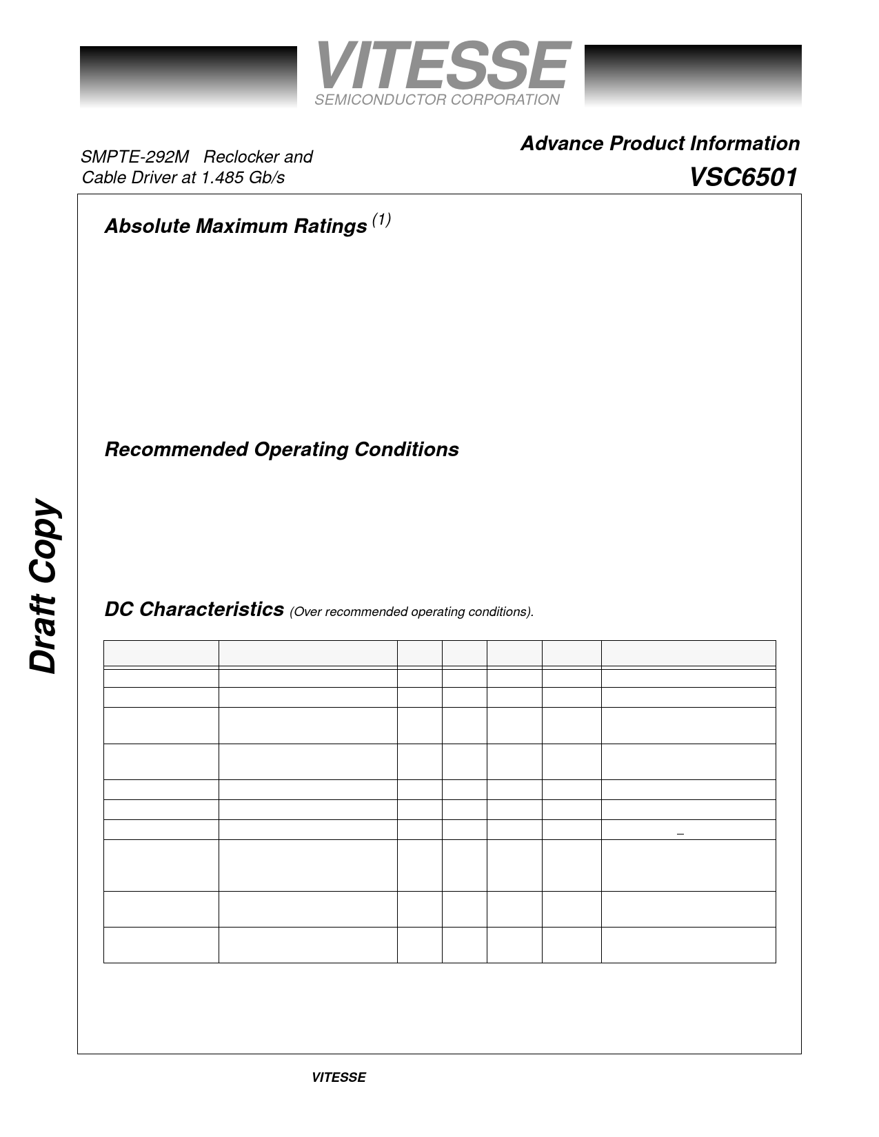
Absolute Maximum Ratings (1)
Power Supply Voltage (VDD) .............................................................................................................-0.5V to +4V
PECL DC Input Voltage ......................................................................................................... -0.5V to VDD +0.5V
TTL DC Input Voltage....................................................................................................................... -0.5V to 5.5V
DC Voltage Applied to TTL Outputs ................................................................................... -0.5V to VDD + 0.5V
TTL Output Current ..................................................................................................................................+/-50mA
PECL Output Current ................................................................................................................................+/-50mA
Case Temperature Under Bias .........................................................................................................-55° to +125oC
Storage Temperature.......................................................................................................................-65° to + 150oC
Maximum Input ESD (Human Body Model).............................................................................................. 1500 V
Recommended Operating Conditions
Power Supply Voltage.................................................................................................... ....... ...... ........3.3V +/- 5%
Ambient Operating Temperature Range...............................................................0°C Ambient to +95°C Case
Notes:
1) CAUTION: Stresses listed under “Absolute Maximum Ratings” may be applied to devices one at a time without causing per-
manent damage. Functionality at or above the values listed is not implied. Exposure to these values for extended periods may
affect device reliability.
DC Characteristics (Over recommended operating conditions).
Parameters
VIH
VIL
IIH
IIL
VOH
VOL
VDD
PD
∆VIN
∆VOUT75
Description
Input HIGH voltage (TTL)
Input LOW voltage (TTL)
Input HIGH current (TTL)
Min Typ
2.0 —
0
—
——
Input LOW current (TTL)
Output HIGH Voltage (TTL)
Output LOW Voltage (TTL)
Supply voltage
——
2.4 —
——
3.14 —
Power Dissipation: (Estimated) — 800
PECL input swing:
PECL output swing:
200 —
750 —
Max
5.5
0.8
500
-500
—
0.5
3.47
—
1200
850
Units
V
V
µA
µA
V
V
V
mW
mVp-p
mVp-p
Conditions
—
—
VIN = 2.4 V, 6.8Kohm Pull-up
resistor on all inputs.
VIN = 0.5 V, 6.8Kohm Pull-up
resistor on all inputs.
IOH = -1.0mA
IOL= +1.0mA
VDD = 3.3V + 5%
Outputs open, VDD = VDD
max
(These are estimates)
AC Coupled.
Internally biased at VDD/2
Using appropriate termination
network
Page 6
© VITESSE SEMICONDUCTOR CORPORATION
741 Calle Plano, Camarillo, CA 93012 • 805/388-3700 • FAX: 805/987-5896
G52310-0, Rev. 2.0
4/10/00
Share Link: 