AD8072JR-REEL 查看數據表(PDF) - Analog Devices
零件编号
产品描述 (功能)
生产厂家
AD8072JR-REEL Datasheet PDF : 13 Pages
| |||
AD8072/AD8073
APPLICATIONS
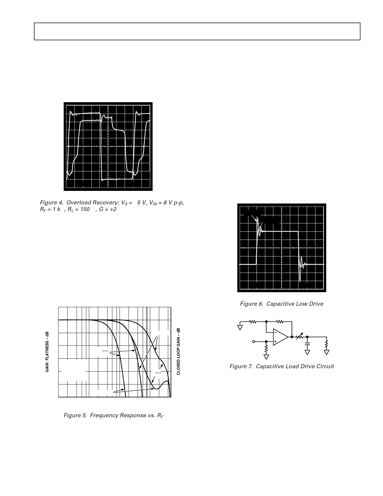
Overdrive Recovery
Overdrive of an amplifier occurs when the output and/or input
range are exceeded. The amplifier must recover from this overdrive
condition and resume normal operation. As shown in Figure 4,
the AD8072 and AD8073 recover within 75 ns from positive
overdrive and 30 ns from negative overdrive.
VIN
VOUT
1V
25ns
Figure 4. Overload Recovery; VS = ±5 V, VIN = 8 V p-p,
RF = 1 kΩ, RL = 150 Ω, G = +2
Bandwidth vs. Feedback Resistor Value
The closed-loop frequency response of a current feedback amplifier
is a function of the feedback resistor. A smaller feedback resistor
will produce a wider bandwidth response. However, if the feed-
back resistance becomes too small, the gain flatness can be
affected. As a practical consideration, the minimum value of
feedback resistance for the AD8072/AD8073 was found to be
649 Ω. For resistances below this value, the gain flatness will be
affected and more significant lot-to-lot variations in device per-
formance will be noticed. Figure 5 shows a plot of the frequency
response of an AD8072/AD8073 at a gain of two with both feed-
back and gain resistors equal to 649 Ω.
6.1
7
6.0
6
5.9
RF = 649⍀ 5
5.8
5.7
VS = ؎5V
AV = 2
5.6 RL = 150⍀
VO = 0.2V p-p
5.5
0.1 dB
DIV
4
3
1 dB
2
DIV
1
5.4
0.1
RF = 2k⍀
1
10
100
FREQUENCY – MHz
0
500
Figure 5. Frequency Response vs. RF
On the other hand, the bandwidth of a current feedback ampli-
fier can be decreased by increasing the feedback resistance. This
can sometimes be useful where it is desired to reduce the noise
bandwidth of a system. As a practical matter, the maximum
value of feedback resistor was found to be 2 kΩ. Figure 5 shows
the frequency response of an AD8072/AD8073 at a gain of two
with both feedback and gain resistors equal to 2 kΩ.
Capacitive Load Drive
When an op amp output drives a capacitive load, extra phase shift
due to the pole formed by the op amp’s output impedance and
the capacitor can cause peaking or even oscillation. The top trace
of Figure 6, RS = 0 Ω, shows the output of one of the amplifiers of
the AD8072/AD8073 when driving a 50 pF capacitor as shown in
the schematic of Figure 7.
The amount of peaking can be significantly reduced by adding
a resistor in series with the capacitor. The lower trace of Figure 6
shows the same capacitor being driven with a 25 Ω resistor
in series with it. In general, the resistor value will have to be
experimentally determined, but 10 Ω to 50 Ω is a practical range
of values to experiment with for capacitive loads of up to a few
hundred pF.
RS = 0Ω
RS = 25Ω
50mV
20ns
Figure 6. Capacitive Low Drive
1k⍀
1k⍀
VIN = 100mV p-p
50⍀
RS
CL
50pF
RL
1k⍀
Figure 7. Capacitive Load Drive Circuit
REV. D
–9–
Share Link: 