LTC1144 查看數據表(PDF) - Linear Technology
零件编号
产品描述 (功能)
生产厂家
LTC1144 Datasheet PDF : 12 Pages
| |||
LTC1144
Applications Information
theory will explain how the LTC1144 behaves. The loss,
and hence the efficiency, is set by the output impedance.
As frequency is decreased, the output impedance will
eventually be dominated by the 1/(f × C1) term and power
efficiency will drop.
9I
BOOST
(1)
V+
I
Note also that power efficiency decreases as frequency
goes up. This is caused by internal switching losses which
occur due to some finite charge being lost on each switching
cycle. This charge loss per unit cycle, when multiplied by
the switching frequency, becomes a current loss. At high
frequency this loss becomes significant and the power
efficiency starts to decrease.
9I
GND
(3)
OSC SCHMITT
(7) TRIGGER
≈20pF
I
1144 F06
100 V+ = 15V, C1 = C2 = 10µF
600
IL = 20mA, TA = 25°C
95
500
POWER
90
CONVERSION
400
EFFICIENCY
85
300
80
200
OUTPUT
75
RESISTANCE
100
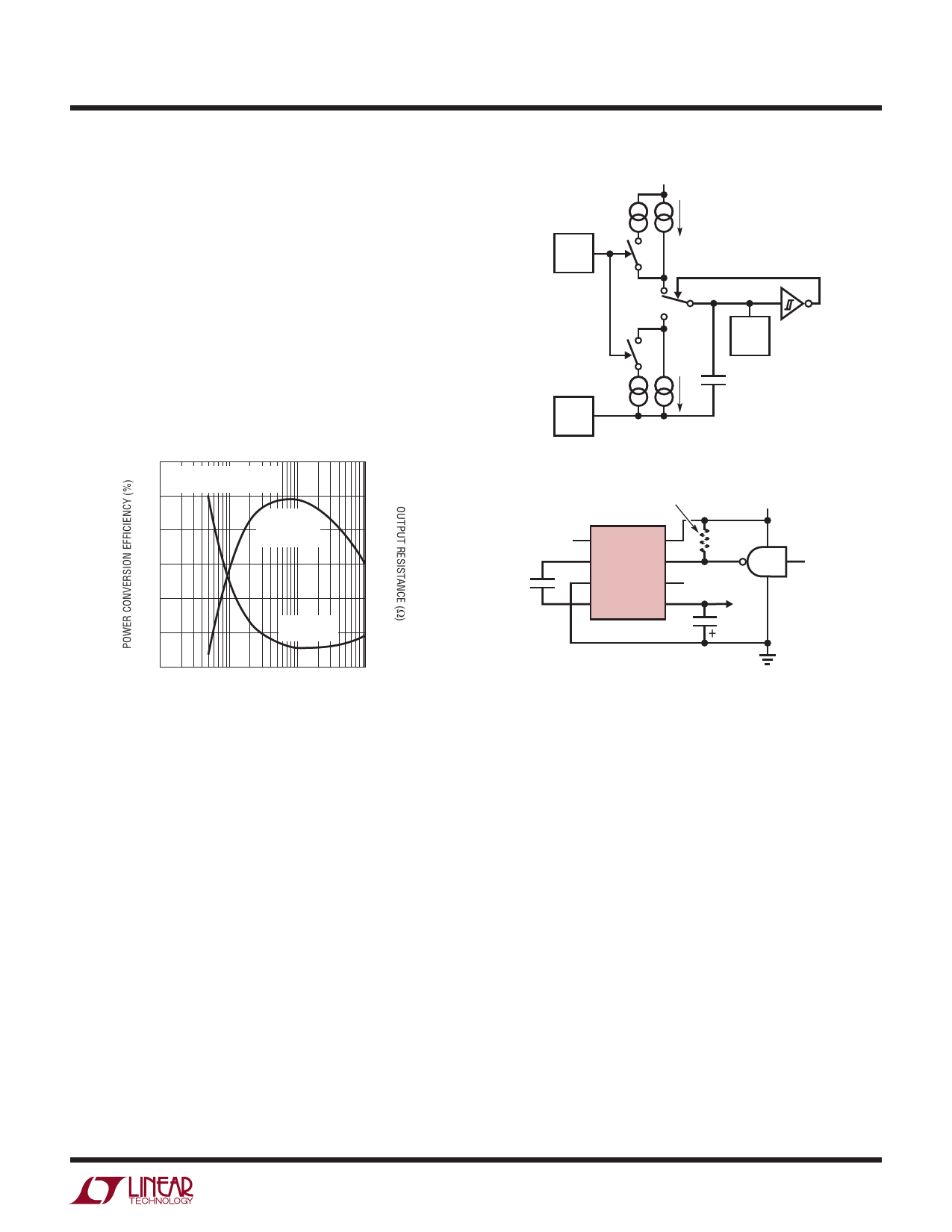
Figure 6. Oscillator
+
C1
NC 1
2
3
4
REQUIRED FOR
TTL LOGIC
8
7
LTC1144 6
5
V+
100k
– (V +)
C2
OSC INPUT
1144 F07
70
0.1
0
1
10
100
OSCILLATOR FREQUENCY (kHz)
1144 F05
Figure 5. Power Conversion Efficiency and Output
Resistance vs Oscillator Frequency
SHDN (Pin 6)
The LTC1144 has a SHDN pin that will disable the internal
oscillator when it is pulled low. The supply current will
also drop to 8µA.
OSC (Pin 7) and Boost (Pin 1)
The switching frequency can be raised, lowered or driven
from an external source. Figure 6 shows a functional
diagram of the oscillator circuit.
By connecting the boost pin (pin 1) to V+, the charge and
discharge current is increased, and hence the frequency
is increased by approximately 10 times. Increasing the
frequency will decrease output impedance and ripple for
higher load currents.
Loading pin 7 with more capacitance will lower the
Figure 7. External Clocking
frequency. Using the boost (pin 1) in conjunction with
external capacitance on pin 7 allows user selection of the
frequency over a wide range.
Driving the LTC1144 from an external frequency source
can be easily achieved by driving pin 7 and leaving the
boost pin open as shown in Figure 7. The output current
from pin 7 is small, typically 4µA, so a logic gate is capable
of driving this current. The choice of using a CMOS logic
gate is best because it can operate over a wide supply
voltage range (3V to 15V) and has enough voltage swing
to drive the internal Schmitt trigger shown in Figure 6. For
5V applications, a TTL logic gate can be used by simply
adding an external pull-up resistor (see Figure 7).
Capacitor Selection
External capacitors C1 and C2 are not critical. Matching is
not required, nor do they have to be high quality or tight
tolerance. Aluminum or tantalum electrolytics are excellent
choices, with cost and size being the only consideration.
1144fa
For more information www.linear.com/LTC1144
7
Share Link: 