LT1306 查看數據表(PDF) - Linear Technology
零件编号
产品描述 (功能)
生产厂家
LT1306 Datasheet PDF : 16 Pages
| |||
LT1306
PIN FUNCTIONS
VC (Pin 1): Compensation Pin for Error Amplifier. VC is
the output of the transconductance error amplifier. Loop
frequency compensation is done by connecting an RC
network from the VC pin to ground.
FB (Pin 2): Inverting Input of the Error Amplifier. Connect
the resistor divider tap here. Set output voltage according
to VOUT = 1.24V (1 + R1/R2).
VOUT (Pin 3): Output of the Switching Regulator and Emit-
ter of the Synchronous Rectifier. Connect appropriate
output capacitor from here to ground. VOUT must be kept
below 5.5V.
GND (Pin 4): Ground. Connect to local ground plane.
SW (Pin 5): Switch Pin. The collectors of the grounded
power switch and the synchronous rectifier. Keep the SW
trace as short as possible to minimize EMI.
CAP (Pin 6): Power Supply to the Synchronous Rectifier
Driver. The bootstrap capacitor and the blocking diode
are tied to this pin. The CAP voltage switches between a
low level of VIN – VD to a high level determined by the VSW
high level.
VIN (Pin 7): Supply or Battery Input Pin. Must be closely
bypassed to ground plane.
S/S (Pin 8): Shutdown and Synchronization Pin. Shut-
down is active low with a typical threshold of 0.9V. For
normal operation, the S/S pin is tied to VIN. To externally
synchronize the switching regulator, drive the S/S pin
with a pulse train.
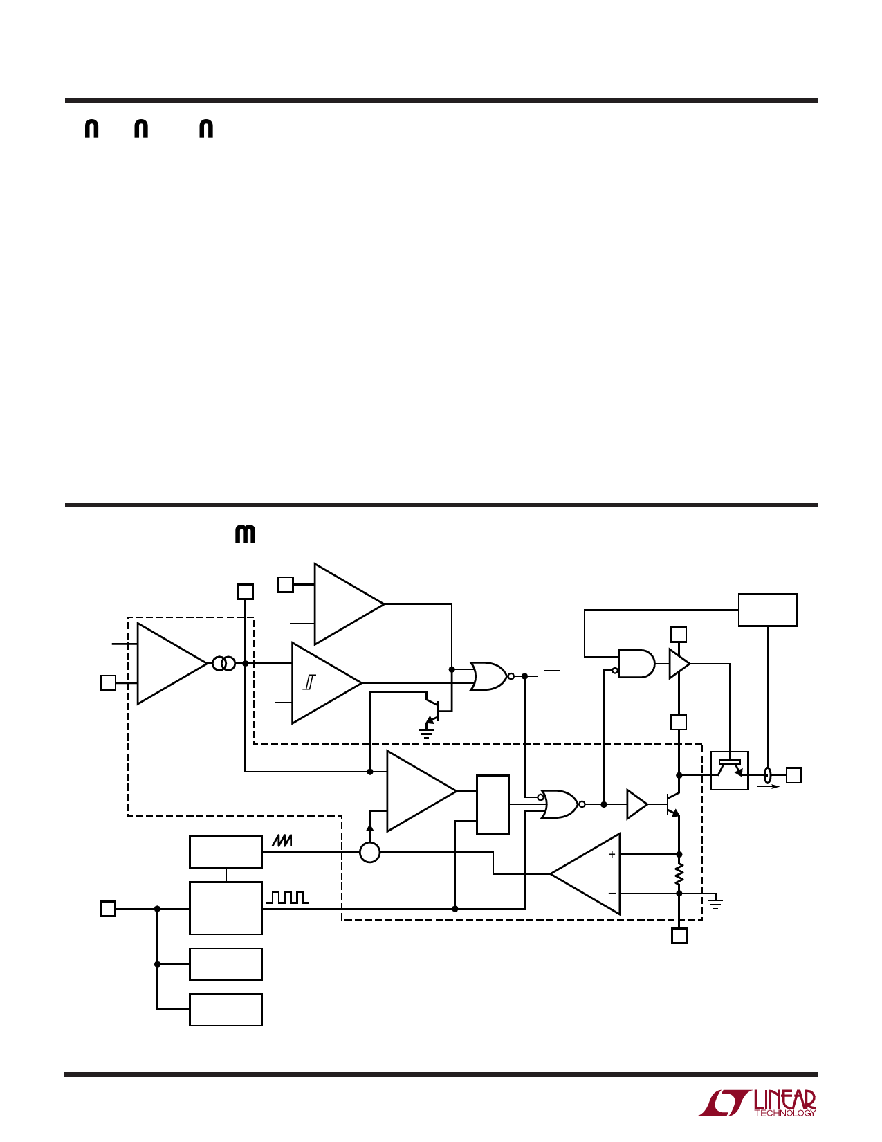
BLOCK DIAGRA
1.24V
FB 2
+
A1
gm
–
VC
VIN
7
1
1.65V
–
A5
+
–
A3
VB +
S/S 8
RAMP
COMPENSATION
300kHz OSC
SYNC
SHDN
REF/BIAS
–
A4
+
++
Σ
CLK
UVLO
X4
IRECT > 0
X3
IDLE
CAP
6
X5
DCM
CONTROL
X1
S
Q
R
5 SW
OUT
Q2
3
X2
X4
Q1
RECTIFIER IRECT
+VCE2–
A2
SENSE
RS
AMP
PWM CONTROL
4 1306 F02
GND
SHUTDOWN
DELAY
Figure 2. LT1306 Block Diagram
6
Share Link: 