MC145745FW 查看數據表(PDF) - Motorola => Freescale
零件编号
产品描述 (功能)
生产厂家
MC145745FW Datasheet PDF : 16 Pages
| |||
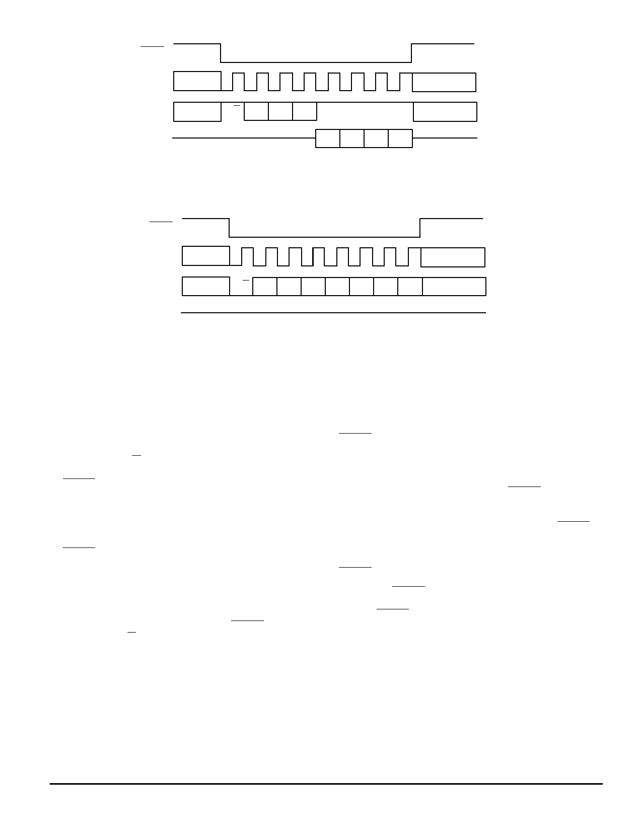
SCPEN
ÎÎÎÎ SCPCLK
ÎÎÎÎÎÎÎÎÎÎÎÎ SCP Rx
R/W A2 A1 A0
ÎÎÎÎÎ DON’T CARE
ÎÎÎÎÎÎÎÎÎÎÎÎÎÎÎ DON’T CARE
SCP Tx
HIGH IMPEDANCE
D3 D2 D1 D0
Figure 5. Serial Control Port Read Operation
SCPEN
ÎÎÎÎ ÎÎÎÎÎ SCPCLK
ÎÎÎÎÎÎÎÎÎÎÎÎ ÎÎÎÎÎÎÎÎÎÎÎÎÎÎÎ SCPRx
DON’T CARE
R/W A2 A1 A0 D3 D2 D1 D0 DON’T CARE
SCP Tx
HIGH IMPEDANCE
Figure 6. Serial Control Port Write Operation
DESCRIPTION OF THE SCP TERMINAL
The SCP bus is made up of the following four pins.
SCP Tx (Pin 20)
The SCP Tx pin outputs the control, status, and data in-
formation from the 4–bit wide register. During the read action
transaction, a R/W bit and the three address bits are shifted
in from SCP Rx at four SCPCLK rising edges, subsequent to
SCPEN going low. After this, if a read operation is selected,
SCP Tx comes out of the high impedance state at the first
falling edge of SCPCLK, and outputs the first bit (MSB) of the
chosen register. The remaining three bits of the chosen reg-
ister are shifted out from SCP Tx at the following three
SCPCLK falling edges. After the last bit (LSB) is shifted out,
SCPEN must return to high. Then SCP Tx returns to the high
impedance condition.
SCP Rx (Pin 21)
The SCP Rx pin is used to input control and data informa-
tion into the 4–bit wide register. Data is shifted in from
SCP Rx at SCPCLK rising edge, while SCPEN is low. The
first bit is the R/W bit (1 = read, 0 = write), and the next three
bits address one of seven byte–registers. The address bits
are shifted in MSB first. If the write action is chosen, the 4–bit
data is shifted in from SCP Rx at the next four SCPCLK rising
edges. If the read action is chosen, 4–bit data in the selected
register is shifted out on SCP Tx. SCP Rx is ignored while
SCPEN is high.
SCPCLK (Pin 22)
The SCPCLK pin is an input of standard clock for hand-
shaking between SCP and MCU. After SCPEN comes low
and the SCP transaction occurs, data is shifted from SCP Rx
into the device at the rising edge of SCPCLK, and is shifted
out on SCP Tx at the falling edge of SCPCLK. When SCPEN
is high, SCPCLK is ignored (i.e., it may be continuous or it
can operate in the burst mode).
SCPEN (Pin 23)
When the SCPEN pin is held low, the SCP transaction is
enabled and control, status, and data information is trans-
ferred. If SCPEN is returned to high, the SCP action in prog-
ress is aborted, and the SCP Tx pin enters a high impedance
condition.
MC145745
10
MOTOROLA
Share Link: 