AD7834 查看數據表(PDF) - Analog Devices
零件编号
产品描述 (功能)
生产厂家
AD7834 Datasheet PDF : 28 Pages
| |||
AD7834/AD7835
44 43 42 41 40 39 38 37 36 35 34
NC 1
DSGA 2
VOUT1 3
VOUT2 4
NC 5
A2 6
A1 7
A0 8
CLR 9
LDAC 10
BYSHF 11
PIN 1
IDENTIFIER
AD7835
TOP VIEW
(Not to Scale)
33 NC
32 DSGB
31 VOUT3
30 VOUT4
29 DB13
28 DB12
27 DB11
26 DB10
25 DB9
24 DB8
23 DB7
12 13 14 15 16 17 18 19 20 21 22
NC = NO CONNECT
Figure 7. AD7835 MQFP Pin Configuration
NC 7
DSGA 8
VOUT1 9
VOUT2 10
NC 11
A2 12
A1 13
A0 14
CLR 15
LDAC 16
BYSHF 17
6 5 4 3 2 1 44 43 42 41 40
PIN 1
IDENTIFIER
AD7835
TOP VIEW
(Not to Scale)
39 NC
38 DSGB
37 VOUT3
36 VOUT4
35 DB13
34 DB12
33 DB11
32 DB10
31 DB9
30 DB8
29 DB7
18 19 20 21 22 23 24 25 26 27 28
NC = NO CONNECT
Figure 8. AD7835 PLCC Pin Configuration
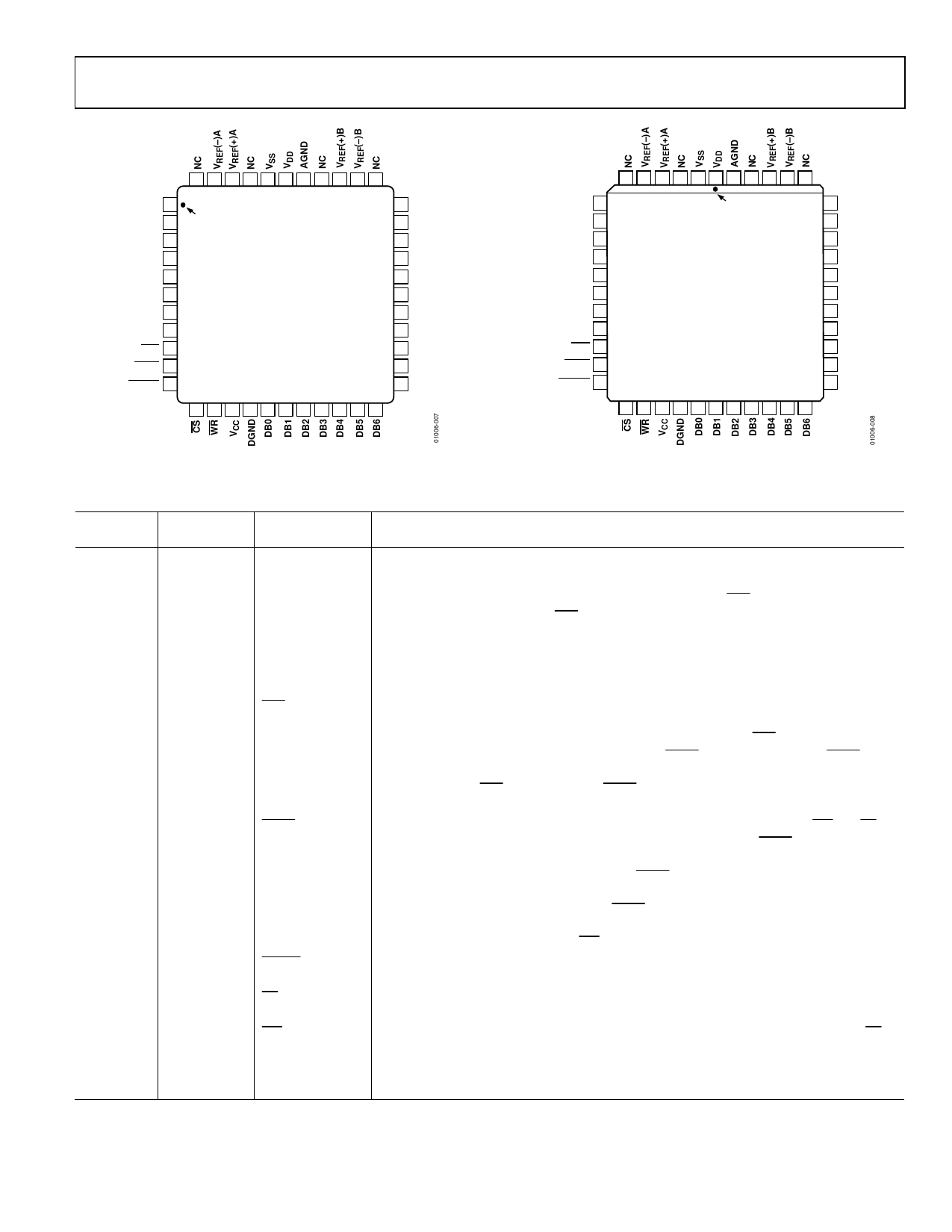
Table 8. AD7835 Pin Function Descriptions
Pin No.
MQFP
Pin No. PLCC Pin Mnemonic
1, 5, 33, 34, 3, 6, 7, 11, 39, NC
37, 41, 44 40, 43
2
8
DSGA
3, 4, 31, 30 9, 10, 37, 36
8, 7, 6
14, 13, 12
9
15
VOUT1 to VOUT4
A0, A1, A2
CLR
10
16
LDAC
11
17
12
18
13
19
14
20
15
21
BYSHF
CS
WR
VCC
DGND
Description
No Connect.
Device Sense Ground A Input. Used in conjunction with the CLR input for power-on
protection of the DACs. When CLR is low, DAC outputs VOUT1 and VOUT2 are forced to the
potential on the DSGA pin.
DAC Outputs.
Address Inputs. A0 and A1 are decoded to select one of the four input latches for a data
transfer. A2 is used to select all four DACs simultaneously.
Asynchronous Clear Input (Level Sensitive, Active Low). When this input is brought low,
all analog outputs are switched to the externally set potentials on the DSG pins (VOUT1
and VOUT2 follow DSGA, and VOUT3 and VOUT4 follow DSGB). When CLR is brought high, the
signal outputs remain at the DSG potentials until LDAC is brought low. When LDAC is
brought low, the analog outputs are switched back to reflect their individual DAC output
levels. As long as CLR remains low, the LDAC signals are ignored, and the signal outputs
remain switched to the potential on the DSG pins.
Load DAC Input (Level Sensitive). This input signal, in conjunction with the WR and CS
input signals, determines how the analog outputs are updated. If LDAC is maintained
high while new data is being loaded into the device’s input registers, no change occurs
on the analog outputs. Subsequently, when LDAC is brought low, the contents of all four
input registers are transferred into their respective DAC latches, updating the analog
outputs simultaneously. Alternatively, if LDAC is brought low while new data is being
entered, the addressed DAC latch and corresponding analog output are updated
immediately on the rising edge of WR.
Byte Shift Input. When low, it shifts the data on DB0 to DB7 into the DB8 to DB13 half of
the input register.
Level-Triggered Chip Select Input (Active Low). The device is selected when this input is
low.
Level-Triggered Write Input (Active Low). When active, it is used in conjunction with CS
to write data over the input databus.
Logic Power Supply: 5 V ± 5%.
Digital Ground.
Rev. D | Page 9 of 28
Share Link: 