HGT1S12N60C3S 查看數據表(PDF) - Fairchild Semiconductor
零件编号
产品描述 (功能)
生产厂家
HGT1S12N60C3S Datasheet PDF : 7 Pages
| |||
HGTP12N60C3, HGT1S12N60C3S
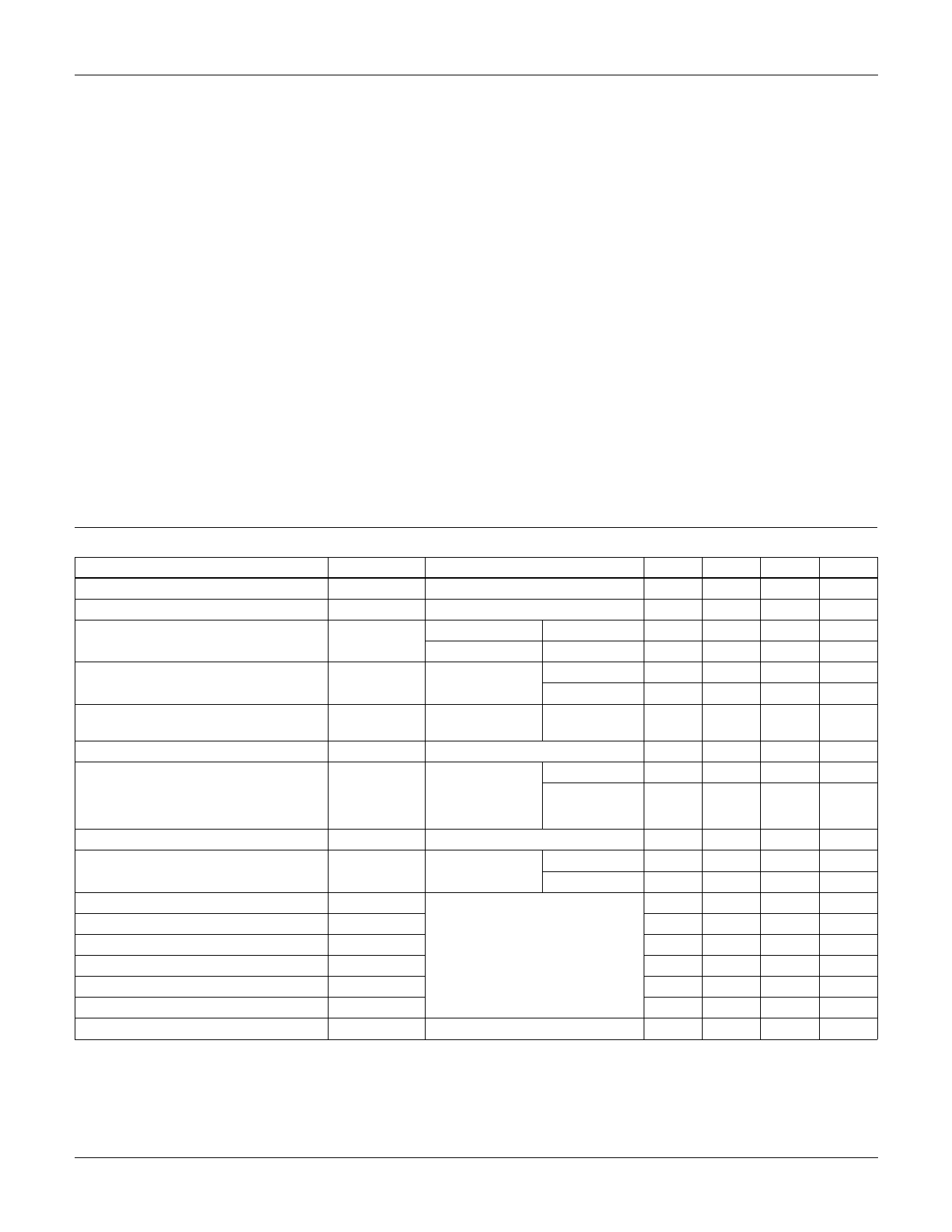
Absolute Maximum Ratings TC = 25oC, Unless Otherwise Specified
Collector to Emitter Voltage . . . . . . . . . . . . . . . . . . . . . . . . . . . . . . . . . . . . . . . . . . . . . . BVCES
Collector Current Continuous
At TC = 25oC . . . . . . . . . . . . . . . . . . . . . . . . . . . . . . . . . . . . . . . . . . . . . . . . . . . . . . . . . IC25
At TC = 110oC . . . . . . . . . . . . . . . . . . . . . . . . . . . . . . . . . . . . . . . . . . . . . . . . . . . . . . . IC110
Collector Current Pulsed (Note 1) . . . . . . . . . . . . . . . . . . . . . . . . . . . . . . . . . . . . . . . . . . . ICM
Gate to Emitter Voltage Continuous. . . . . . . . . . . . . . . . . . . . . . . . . . . . . . . . . . . . . . . . . VGES
Gate to Emitter Voltage Pulsed . . . . . . . . . . . . . . . . . . . . . . . . . . . . . . . . . . . . . . . . . . . . VGEM
Switching Safe Operating Area at TJ = 150oC (Figure 14) . . . . . . . . . . . . . . . . . . . . . . SSOA
Power Dissipation Total at TC = 25oC . . . . . . . . . . . . . . . . . . . . . . . . . . . . . . . . . . . . . . . . . PD
Power Dissipation Derating TC > 25oC . . . . . . . . . . . . . . . . . . . . . . . . . . . . . . . . . . . . . . . . . .
Reverse Voltage Avalanche Energy . . . . . . . . . . . . . . . . . . . . . . . . . . . . . . . . . . . . . . . . EARV
Operating and Storage Junction Temperature Range . . . . . . . . . . . . . . . . . . . . . . . . TJ, TSTG
Maximum Lead Temperature for Soldering . . . . . . . . . . . . . . . . . . . . . . . . . . . . . . . . . . . . . TL
Short Circuit Withstand Time (Note 2) at VGE = 15V. . . . . . . . . . . . . . . . . . . . . . . . . . . . . . tSC
Short Circuit Withstand Time (Note 2) at VGE = 10V. . . . . . . . . . . . . . . . . . . . . . . . . . . . . . tSC
HGTP12N60C3, HGT1S12N60C3S
600
24
12
96
±20
±30
24A at 600V
104
0.83
100
-40 to 150
260
4
13
UNITS
V
A
A
A
V
V
W
W/oC
mJ
oC
oC
µs
µs
CAUTION: Stresses above those listed in “Absolute Maximum Ratings” may cause permanent damage to the device. This is a stress only rating and operation of the
device at these or any other conditions above those indicated in the operational sections of this specification is not implied.
NOTES:
1. Repetitive Rating: Pulse width limited by maximum junction temperature.
2. VCE(PK) = 360V, TJ = 125oC, RG = 25Ω.
Electrical Specifications TC = 25oC, Unless Otherwise Specified
PARAMETER
SYMBOL
TEST CONDITIONS
MIN
TYP
MAX UNITS
Collector to Emitter Breakdown Voltage
Emitter-Collector Breakdown Voltage
Collector to Emitter Leakage Current
Collector to Emitter Saturation Voltage
Gate to Emitter Threshold Voltage
Gate to Emitter Leakage Current
Switching SOA
BVCES
IC = 250µA, VGE = 0V
600
-
-
V
BVECS
ICES
VCE(SAT)
VGE(TH)
IC = 10mA, VGE = 0V
VCE = BVCES
TC = 25oC
VCE = BVCES
TC = 150oC
IC = IC110,
TC = 25oC
VGE = 15V
TC = 150oC
IC = 250µA,
TC = 25oC
VCE = VGE
24
30
-
V
-
-
250
µA
-
-
1.0
mA
-
1.65
2.0
V
-
1.85
2.2
V
3.0
5.0
6.0
V
IGES
SSOA
VGE = ±20V
TJ = 150oC
RG = 25Ω
VGE = 15V
L = 100µH
-
VCE(PK) = 480V
80
VCE(PK) = 600V
24
-
±100
nA
-
-
A
-
-
A
Gate to Emitter Plateau Voltage
On-State Gate Charge
Current Turn-On Delay Time
Current Rise Time
Current Turn-Off Delay Time
Current Fall Time
Turn-On Energy
Turn-Off Energy (Note 3)
Thermal Resistance
NOTE:
VGEP
QG(ON)
td(ON)I
trI
td(OFF)I
tfI
EON
EOFF
RθJC
IC = IC110, VCE = 0.5 BVCES
IC = IC110,
VGE = 15V
VCE = 0.5 BVCES VGE = 20V
TJ = 150oC,
ICE = IC110,
VCE(PK) = 0.8 BVCES,
VGE = 15V,
RG = 25Ω,
L = 100µH
-
7.6
-
V
-
48
55
nC
-
62
71
nC
-
14
-
ns
-
16
-
ns
-
270
400
ns
-
210
275
ns
-
380
-
µJ
-
900
-
µJ
-
-
1.2
oC/W
3. Turn-Off Energy Loss (EOFF) is defined as the integral of the instantaneous power loss starting at the trailing edge of the input pulse and ending
at the point where the collector current equals zero (ICE = 0A). The HGTP12N60C3 and HGT1S12N60C3S were tested per JEDEC standard
No. 24-1 Method for Measurement of Power Device Turn-Off Switching Loss. This test method produces the true total Turn-Off Energ y Loss.
Turn-On losses include diode losses.
©2001 Fairchild Semiconductor Corporation
HGTP12N60C3, HGT1S12N60C3S Rev. B
Share Link: 