STK672-010 查看數據表(PDF) - SANYO -> Panasonic
零件编号
产品描述 (功能)
生产厂家
STK672-010 Datasheet PDF : 17 Pages
| |||
STK672-010
Specifications
Absolute Maximum Ratings at Ta = 25°C
Parameter
Maximum supply voltage
Maximum phase output current
Repeat avalanche capacity
Input voltage
Operating substrate temperature
Junction temperature
Storage temperature range
Symbol
VCC1 max
VCC2 max
IOH max
Ear max
No signal
No signal
0.5 s, 1 pulse
VIN max
Tc max
Tj max
Tstg
Conditions
Ratings
Unit
52
V
7.0
V
2.5
A
38
mJ
7.0
V
105
°C
150
°C
–40 to +125
°C
Allowable Operating Ranges at Ta = 25°C
Parameter
Operating supply voltage
Input voltage
Phase drive withstand voltage
Phase current
Symbol
VCC1
VCC2
VIH
VDSS
IOH max
Conditions
With a signal present
With a signal present
Duty: 50% per phase
Electrical Characteristics at Ta = 25°C, VCC1 = 36 V, VCC2 = 5 V
Parameter
Output saturation voltage
Output current (average)
FET diode forward voltage
Current when stopped
On input voltage
Off input voltage
Input leakage current
C1 to C3 high level voltage
C1 to C3 low level voltage
Chopping frequency
Symbol
Vst
Ioave
Vdf
Icco
VIH
VIL
II
CVOH
CVOL
fc
Conditions
RL = 23 Ω
Load (each phase): R = 3.5 Ω, L = 3.8 mH
If = 1.0 A
Pins 14, 15, 16, 17, 18, and 19
Pins 14, 15, 16, 17, 18, and 19
Pins 14, 15, 16, 17, 18, and 19
Pins 1, 2, and 3
Pins 1, 2, and 3
R/C: 2.4 kΩ/6800 pF
Ratings
Unit
18 to 42
V
5 ± 5%
V
0 to VCC2
V
120
V
1.7
A
min
typ
max
Unit
1.1
1.5
V
0.45
0.50
0.59
A
1.2
1.8
V
36
55
mA
4.0
V
1.0
V
–600
+30
µA
2.4
V
0.4
V
35
42
50
kHz
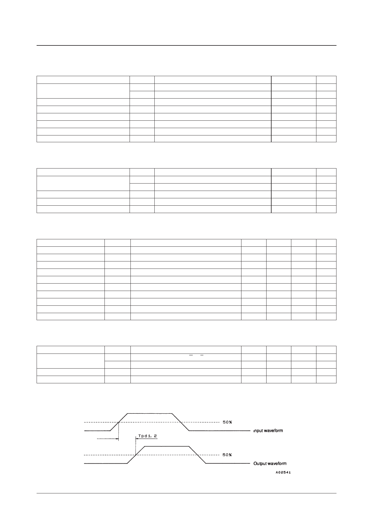
AC Characteristics at Ta = 25°C, VCC1 = 36 V, VCC2 = 5.0 V, CL = 50 pF
Parameter
Symbol
Conditions
min
Delay time
Tpd1
Tpd2
For the clock path: CLK → A, A, B, B
For the clock path: CLK → C1, C2, C3
Output signal interval
Tin
Only for 4-phase 2 excitation
20
Maximum clock frequency
fCLK
Note: Use a rated power supply.
Definition of the Delay Time Tpd
typ
max
Unit
2
µs
2
µs
40
µs
20
kHz
No. 4927-2/17
Share Link: 