SN74LS195AN 查看數據表(PDF) - ON Semiconductor
零件编号
产品描述 (功能)
生产厂家
SN74LS195AN Datasheet PDF : 8 Pages
| |||
SN74LS195A
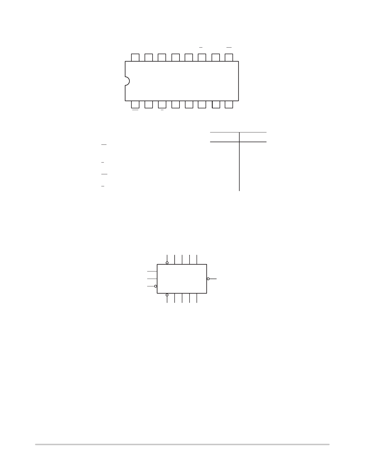
CONNECTION DIAGRAM DIP (TOP VIEW)
VCC Q0 Q1 Q2 Q3 Q3 CP PE
16 15 14 13 12 11 10 9
NOTE:
The Flatpak version has the same
pinouts (Connection Diagram) as
the Dual In-Line Package.
1 2 3 4 56 78
MR J K P0 P1 P2 P3 GND
PIN NAMES
PE
P0 – P3
J
K
CP
MR
Q0 – Q3
Q3
Parallel Enable (Active LOW) Input
Parallel Data Inputs
First Stage J (Active HIGH) Input
First Stage K (Active LOW) Input
Clock (Active HIGH Going Edge) Input
Master Reset (Active LOW) Input
Parallel Outputs
Complementary Last Stage Output
NOTES:
a) 1 TTL Unit Load (U.L.) = 40 mA HIGH/1.6 mA LOW.
LOADING (Note a)
HIGH
LOW
0.5 U.L.
0.5 U.L.
0.5 U.L.
0.5 U.L.
0.5 U.L.
0.5 U.L.
10 U.L.
10 U.L.
0.25 U.L.
0.25 U.L.
0.25 U.L.
0.25 U.L.
0.25 U.L.
0.25 U.L.
5 U.L.
5 U.L.
LOGIC SYMBOL
9456 7
2
J PE P0 P1 P2 P3
10
CP
Q3
11
3
K MR Q0 Q1 Q2 Q3
1 15 14 13 12
VCC = PIN 16
GND = PIN 8
http://onsemi.com
2
Share Link: 