AD698 查看數據表(PDF) - Analog Devices
零件编号
产品描述 (功能)
生产厂家
AD698 Datasheet PDF : 12 Pages
| |||
AD698
Multiply the primary excitation voltage by the VTR to get
the expected secondary voltage at mechanical full scale. For
example, for an LVDT with a sensitivity of 2.4 mV/V/mil and
a full scale of ± 0.1 inch, the VTR = 0.0024 V/V/Mil × 100
mil = 0.24. Assuming the maximum excitation of 3.5 V rms,
the maximum secondary voltage will be 3.5 V rms × 0.24 =
0.84 V rms, which is in the acceptable range.
Conversely the VTR may be measured explicitly. With the
LVDT energized at its typical drive level VPRI, as indicated
by the manufacturer, set the core displacement to its me-
chanical full-scale position and measure the output VSEC of
the secondary. Compute the LVDT voltage transformation
ratio, VTR. VTR = VSEC//VPRI. For the E100, VSEC = 0.72 V
for VPRI = 3 V. VTR = 0.24.
For situations where LVDT sensitivity is low, or the me-
chanical FS is a small fraction of the total stroke length, an
input excitation of more than 3.5 V rms may be needed. In
this case a voltage divider network may be placed across the
LVDT primary to provide smaller voltage for the +BIN and
–BIN input. If, for example, a network was added to divide
the B Channel input by 1/2, then the VTR should also be re-
duced by 1/2 for the purpose of component selection.
Check the power supply voltages by verifying that the peak
values of VA and VB are at least 2.5 volts less than the volt-
ages at +VS and –VS.
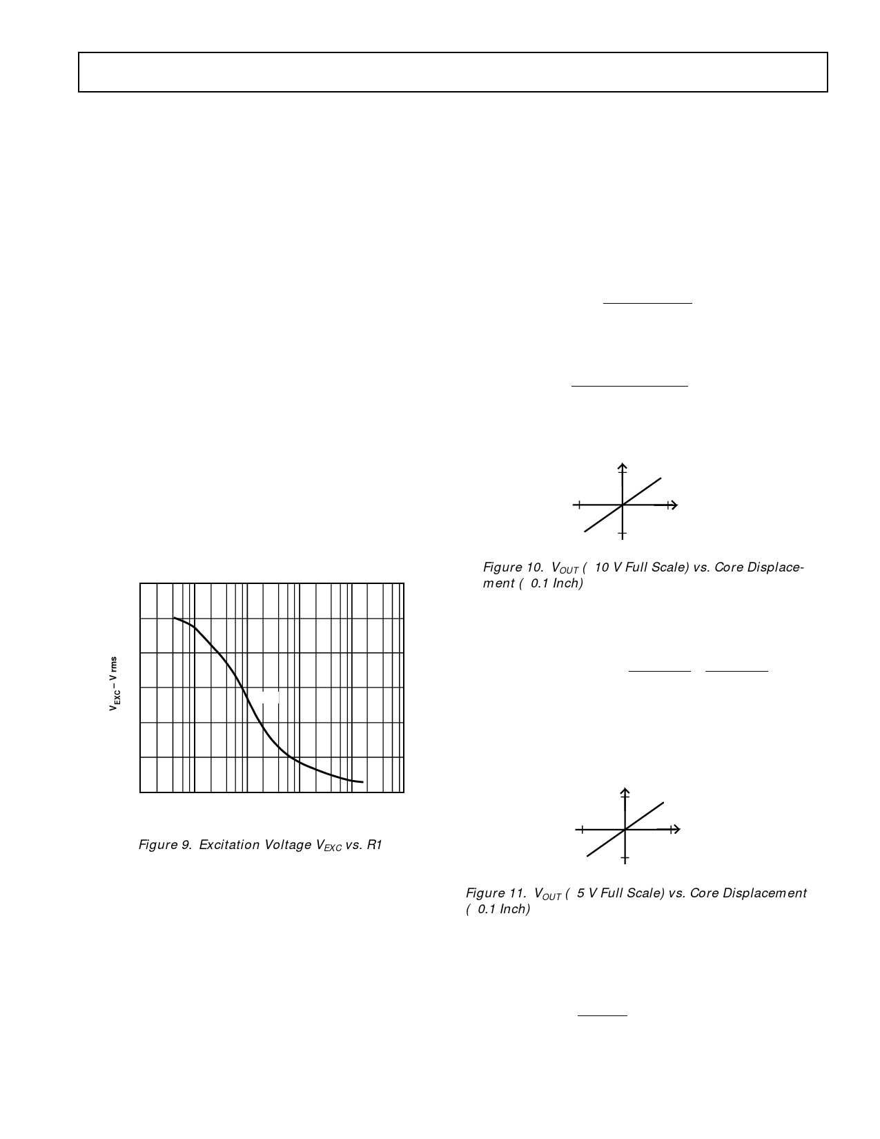
6. Referring to Figure 9, for VS = ± 15 V, select the value of the
amplitude determining component R1 as shown by the curve
in Figure 9.
30
25
20
15
V rms
10
5
0
0.01
0.1
1
10
100
1k
R1 – kΩ
Figure 9. Excitation Voltage VEXC vs. R1
7. C2, C3 and C4 are a function of the desired bandwidth of
the AD698 position measurement subsystem. They should
be nominally equal values.
C2 = C3 = C4 = 10–4 Farad Hz/f5UBSYSTEM (Hz)
If the desired system bandwidth is 250 Hz, then
C2 = C3 = C4 = 10-4 Farad Hz/250 Hz = 0.4 µF
See Figures 14, 15 and 16 for more information about
AD698 bandwidth and phase characterization.
D. Set the Full-Scale Output Voltage
8. To compute R2, which sets the AD698 gain or full-scale
output range, several pieces of information are needed:
a. LVDT sensitivity, S
b. Full-scale core displacement from null, d
S × d = VTR and also equals the ratio A/B at mechanical full
scale. The VTR should be converted to units of V/V.
For a full-scale displacement of d inches, voltage out of the
AD698 is computed as
VOUT = S × d × 500 µA × R2
VOUT is measured with respect to the signal reference,
Pin 21, shown in Figure 7.
Solving for R2,
R2
=
S
×
VOUT
d × 500
µA
(1)
For VOUT = ± 10 V full-scale range (20 V span) and d = ± 0.1
inch full-scale displacement (0.2 inch span)
R2
=
2. 4
×
20 V
0.2 × 500
µA
= 83. 3 kΩ
VOUT as a function of displacement for the above example is
shown in Figure 10.
VOUT (VOLTS)
+10
–0.1
+0.1d (INCHES)
–10
Figure 10. VOUT (±10 V Full Scale) vs. Core Displace-
ment (±0.1 Inch)
E. Optional Offset of Output Voltage Swing
9. Selections of R3 and R4 permit a positive or negative output
voltage offset adjustment.
VOS
=
1.2 V
×
R2
×
R3
1
+2
kΩ
–
R4
1
+2
kΩ
(2)
For no offset adjustment R3 and R4 should be open circuit.
To design a circuit producing a 0 V to +10 V output for a
displacement of +0.1 inch, set VOUT to +10 V, d = 0.2 inch
and solve Equation (1) for R2.
VOUT (VOLTS)
+5
–0.1
+0.1d (INCHES)
–5
Figure 11. VOUT (±5 V Full Scale) vs. Core Displacement
(±0.1 Inch)
This will produce a response shown in Figure 11.
In Equation (2) set VOS = 5 V and solve for R3 and R4. Since a
positive offset is desired, let R4 be open circuit. Rearranging
Equation (2) and solving for R3
R3 = 1.2 × R2 – 2 kΩ = 7.02 kΩ
VOS
REV. B
–7–
Share Link: 