ICS2572 查看數據表(PDF) - Integrated Circuit Systems
零件编号
产品描述 (功能)
生产厂家
ICS2572 Datasheet PDF : 10 Pages
| |||
ICS2572
Digital Inputs
The FS0-FS3 pins and the STROBE pin are used to select the
desired operating frequency of the VCLK output from the 16
pre-programmed/user-programmed selections in the ICS2572.
These pins are also used to load new frequency data into the
registers.
Available configurations for the STROBE input include: posi-
tive-edge triggered, negative-edge triggered, high-level trans-
parent, and low-level transparent (see Ordering Information).
VCLK Output Frequency Selection
To change the VCLK output frequency, simply write the ap-
propriate data to the ICS2572 FS inputs. Do not perform any
further writes to the device for 50 milliseconds (assumes a
14.318 MHz reference). The synthesizer will output the new
frequency programmed into that location after a brief delay
(see timeout specifications).
MCLK Output Frequency Selection
The MS0-MS1 pins are used to directly select the desired
operating frequency of the MCLK output from the four pre-
programmed/user-programmed selections in the ICS2572.
These inputs are not latched, nor are they involved with mem-
ory programming operations.
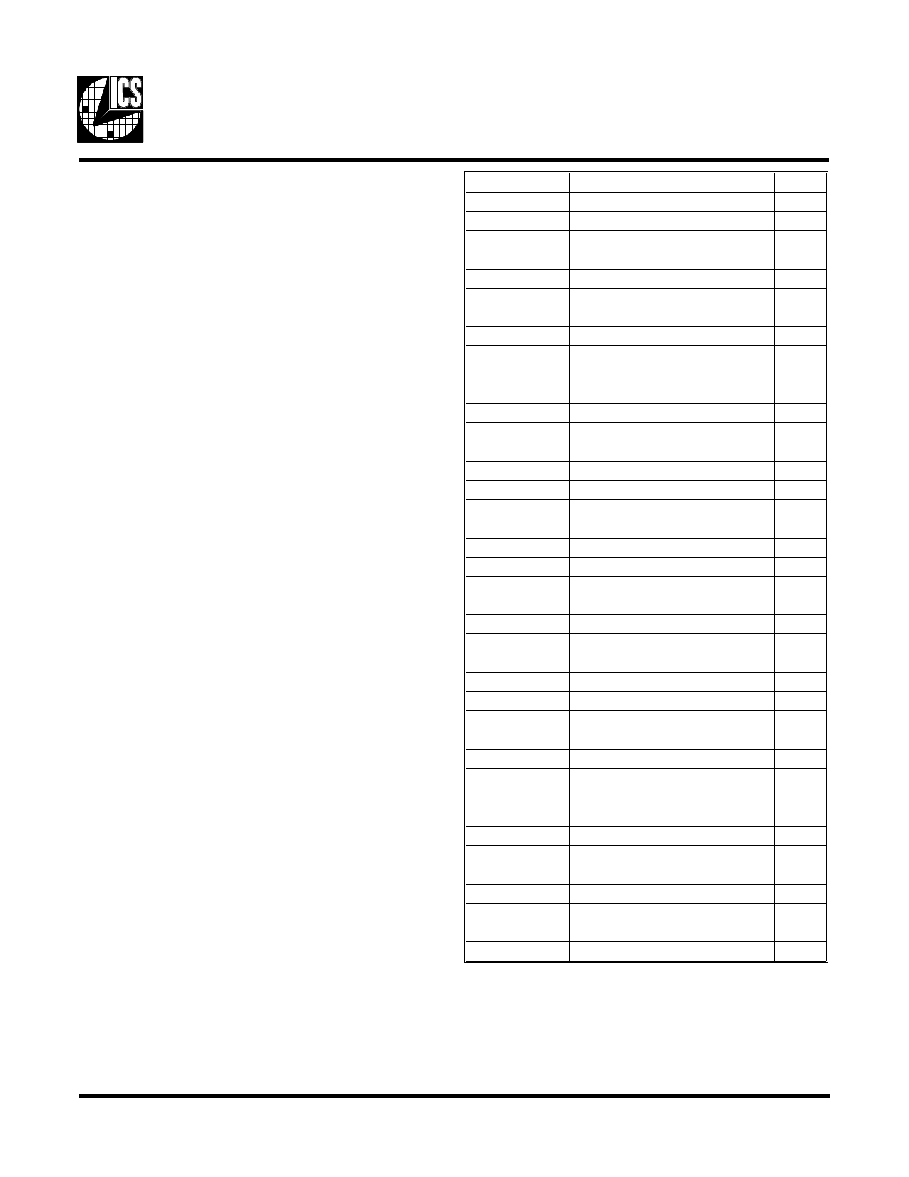
Programming Mode Selection
A programming sequence is defined as a period of at least 50
milliseconds of no data writes to the ICS2572 (to clear the shift
register) followed by a series of data writes (as shown here):
FS0 FS1
FS2
FS3
X
X START bit (must be “0”)
0
X
X
”
1
X
X R/W* control
0
X
X
”
1
X
X L0 (location LSB)
0
X
X
”
1
X
X L1
0
X
X
”
1
X
X L2
0
X
X
”
1
X
X L3
0
X
X
”
1
X
X L4 (location MSB)
0
X
X
”
1
X
X N0 (feedback LSB)
0
X
X
”
1
X
X N1
0
X
X
”
1
X
X N2
0
X
X
”
1
X
X N3
0
X
X
”
1
X
X N4
0
X
X
”
1
X
X N5
0
X
X
”
1
X
X N6
0
X
X
”
1
X
X N7 (feedback MSB)
0
X
X
”
1
X
X EXTFREQ bit (selected if “1”) 0
X
X
”
1
X
X D0 (post-divider LSB)
0
X
X
”
1
X
X D1 (post-divider MSB)
0
X
X
”
1
X
X STOP1 bit (must be “1”
0
X
X
”
1
X
X STOP2 bit (must be “1”)
0
X
X
”
1
E-97
Share Link: 