MX604 查看數據表(PDF) - MX-COM Inc
零件编号
产品描述 (功能)
生产厂家
MX604 Datasheet PDF : 17 Pages
| |||
v.23 Compatible Modem
10
MX604 PRELIMINARY INFORMATION
If the Data Retiming facility is not required, the CLK input to the MX604 should be kept high at all times. The
asynchronous data from the FSK Demodulator will then be connected directly to the RXD output pin, and the
RDY output will not be activated by the FSK signal. This case is illustrated by the example in Figure 8
FSK Demod output :
RXD output :
Received Character 'n'
START 1
2
3
4
5
6
7
8 STOP
START 1
2
3
4
5
6
7
8 STOP
Figure 8: FSK Operation without Rx Data Re-timing (CLK always high)
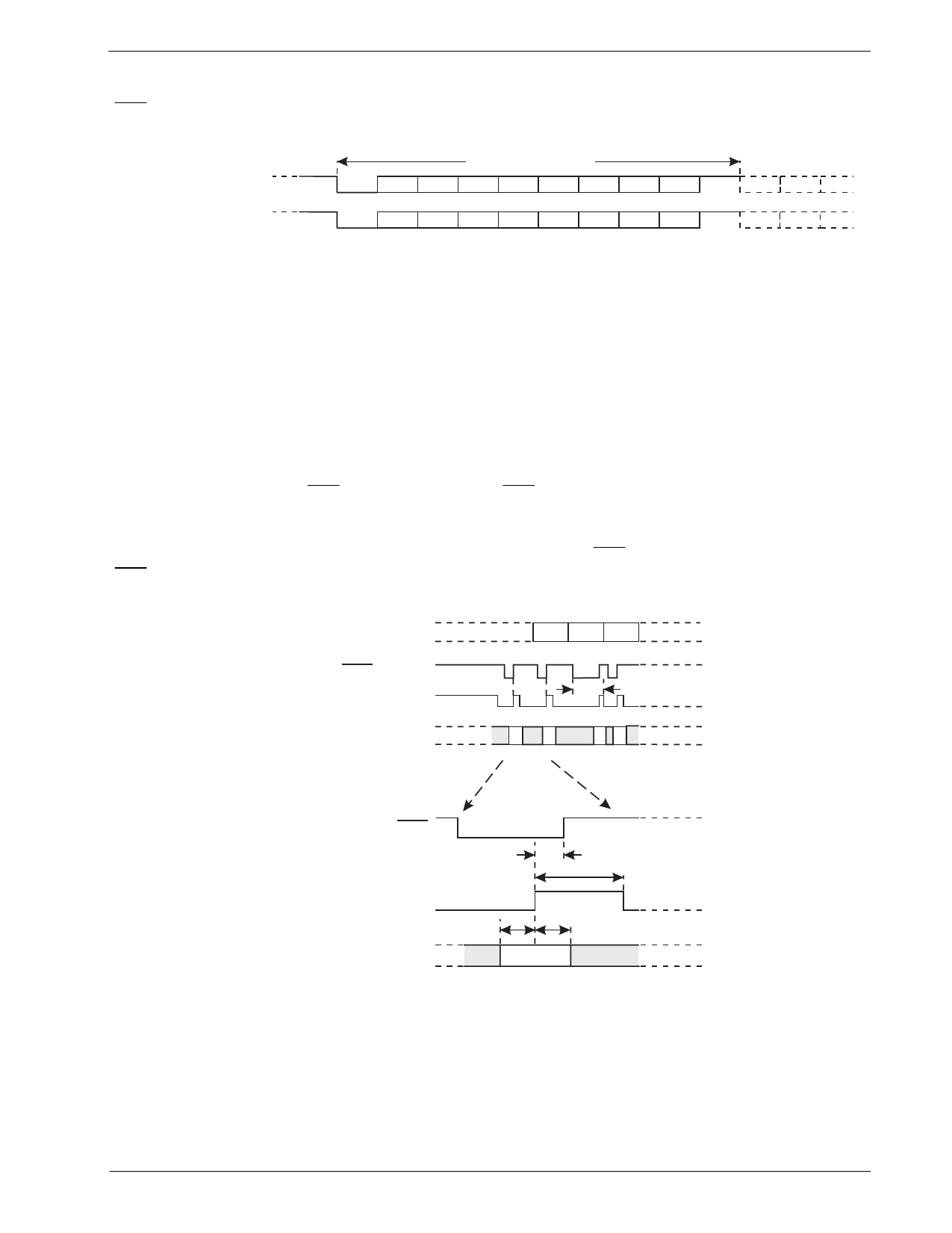
4.9 Tx Data Retiming
The Tx Data Retiming block, when enabled in 1200bps transmit mode, requires the controlling C to load 1 bit
at a time into the device by a pulse applied to the CLK input. The timing of this pulse is not critical. It may be
generated easily by a simple software loop. This facility removes the need for a UART in the C without
incurring an excessive software overhead.
The Tx retiming circuit consists of two 1-bit registers in series, the input of the first is connected to the TXD pin
and the output of the second feeds the FSK modulator. The second register is clocked by an internally
generated 1200Hz signal and when this occurs the CLK input is sampled. If the CLK input is high the TXD pin
directly controls the FSK modulator, if the CLK input is low the FSK modulator is controlled by the output of
the second register and the RDY pin is pulled low. The RDY output is reset by a high level on the CLK input
pin. A low to high change on the CLK input pin will latch the data from the TXD input pin into the first register
ready for transfer to the second register when the internal 1200Hz signal next occurs.
To use the retiming option, the CLK input should be held low until the RDY output is pulled low. When the
RDY pin goes low, the next data bit should be applied to the TXD input and the CLK input pulled high and
then low within the time limits defined in Figure 9.
FSK Modulator input :
123
RDY output :
CLK input :
TXD input :
tR
12
34
RDY
CLK
TXD
tD
tcHI
tS tH
1
tD = Internal MX604 delay; tR = low to CLK going low; tS = data set up time
tcHI = CLK high time, tH = data hold time
Figure 9: FSK Operation with Tx Data Retiming
To ensure synchronization between controlling device and the MX604 when entering Tx retiming mode the
TXD pin must be held at a constant logic level from when the CLK pin is first pulled low to the end of loading
in the second retimed bit. Similarly when exiting Tx retiming mode the TXD pin should be held at the same
logic level as the last retimed bit for at least 2 bit times after the CLK line is pulled high.
1998 MXCOM, INC.
Tele: 800 638 5577 336 744 5050 Fax: 336 744 5054
Doc. # 20480152.004
4800 Bethania Station Road, Winston-Salem, NC 27105-1201 USA
All trademarks and service marks are held by their respective companies.
Share Link: 