MX604 查看數據表(PDF) - MX-COM Inc
零件编号
产品描述 (功能)
生产厂家
MX604 Datasheet PDF : 17 Pages
| |||
v.23 Compatible Modem
9
MX604 PRELIMINARY INFORMATION
4.8 Rx Data Retiming
The Rx Data Retiming function may be used when the received data consists of 1200bps asynchronous
characters, each character consisting of one start bit followed by a minimum of 9 formatted bits as shown in
the table below.
Data bits
7
7
8
8
9
Parity bits
0
1
0
1
0
Stop bits
2
1
1
1
1
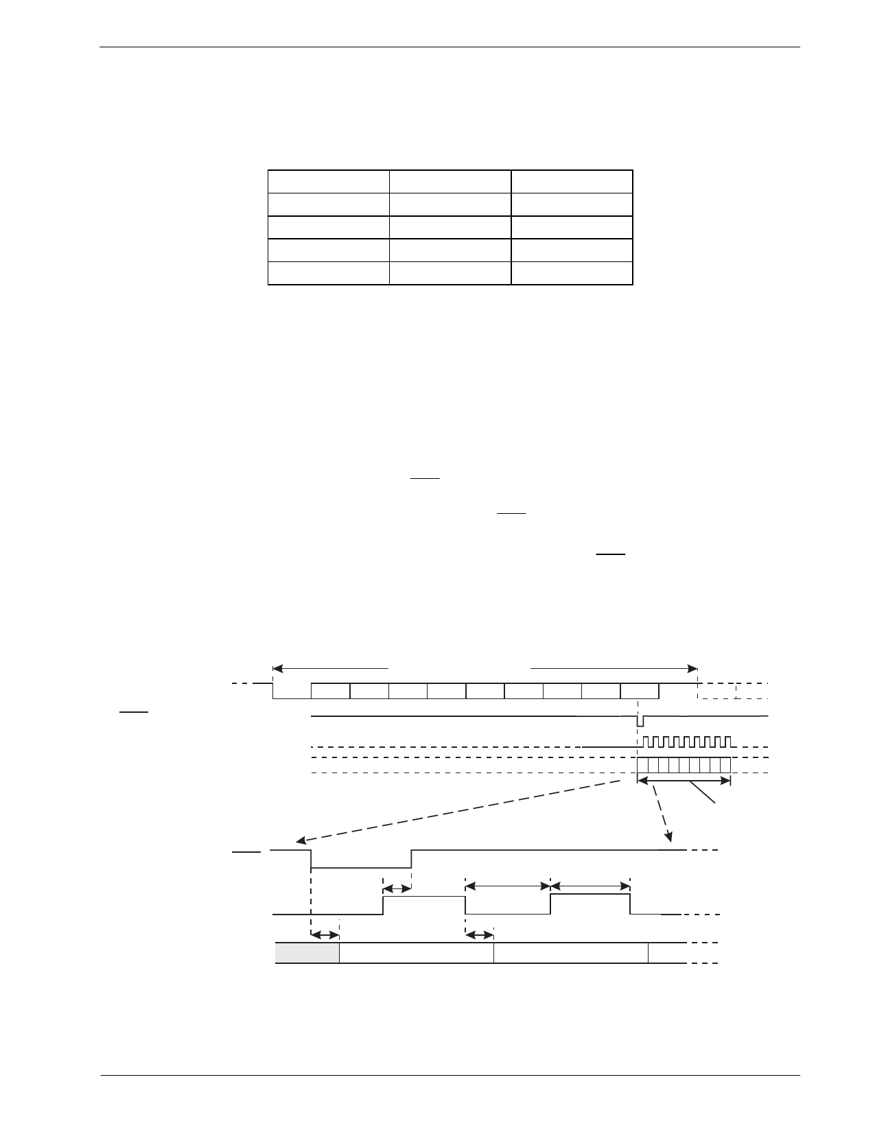
When enabled in receive mode, the Data Retiming block extracts the first 9 bits of each character following
the start bit, from the received asynchronous data stream, and presents them to the C, under the control of
strobe pulses applied to the CLK input. The timing of these pulses is not critical. They may be generated
easily by a simple software loop. This facility removes the need for a UART in the C without incurring an
excessive software overhead.
The receive retiming block consists of two 9-bit shift registers, the input of the first is connected to the output
of the FSK demodulator and the output of the second is connected to the RXD pin. The first register is
clocked by an internally generated signal that stores the 9 received bits following the timing reference of a
high to low transition at the output of the FSK demodulator. When the 9th bit is clocked into the first register
these 9 bits are transferred to the second register, a new stop-start search is initiated and the CLK input is
sampled. If the CLK input is low at this time the RDY pin is pulled low and the first received bit is output on
the RXD pin. The CLK pin should then be pulsed high 9 times, the first 8 high to low transitions will be used
by the device to clock out the bits in the second register. The RDY output is cleared the first time the CLK
input goes high. At the end of the 9th pulse the RXD pin will be connected to the FSK demodulator output.
To use the Data Retiming function, the CLK input should be kept low until the RDY output goes low; if the
Data Retiming function is not required then the CLK input should be kept high at all times.
The only restrictions on the timing of the CLK waveform are those shown in Figure 7 and the need to
complete the transfer of all nine bits into the C within the time of a complete character at 1200bps.
FSK Demod output :
Received Character 'n'
9 Bits of data START 1
2
3
4
5
6
7
8
9 STOP
RDY output :
RXCK input :
RXD output :
1
9
Retimed data bits from
received character 'n'
RDY
RXCK
tD
RXD
tD
tcLO
tcHI
tD
Data Bit 1
Data Bit 2
tD = Internal MX604 delay, tcHI = CLK high time, tcLO = CLK low time
Figure 7: FSK Operation with Rx Data Re-timing
Note: If enabled, the Data Retiming block may interpret speech or other signals as random characters.
1998 MXCOM, INC.
Tele: 800 638 5577 336 744 5050 Fax: 336 744 5054
Doc. # 20480152.004
4800 Bethania Station Road, Winston-Salem, NC 27105-1201 USA
All trademarks and service marks are held by their respective companies.
Share Link: 