AD743JR-16-REEL(2003) 查看數據表(PDF) - Analog Devices
零件编号
产品描述 (功能)
生产厂家
AD743JR-16-REEL Datasheet PDF : 12 Pages
| |||
AD743
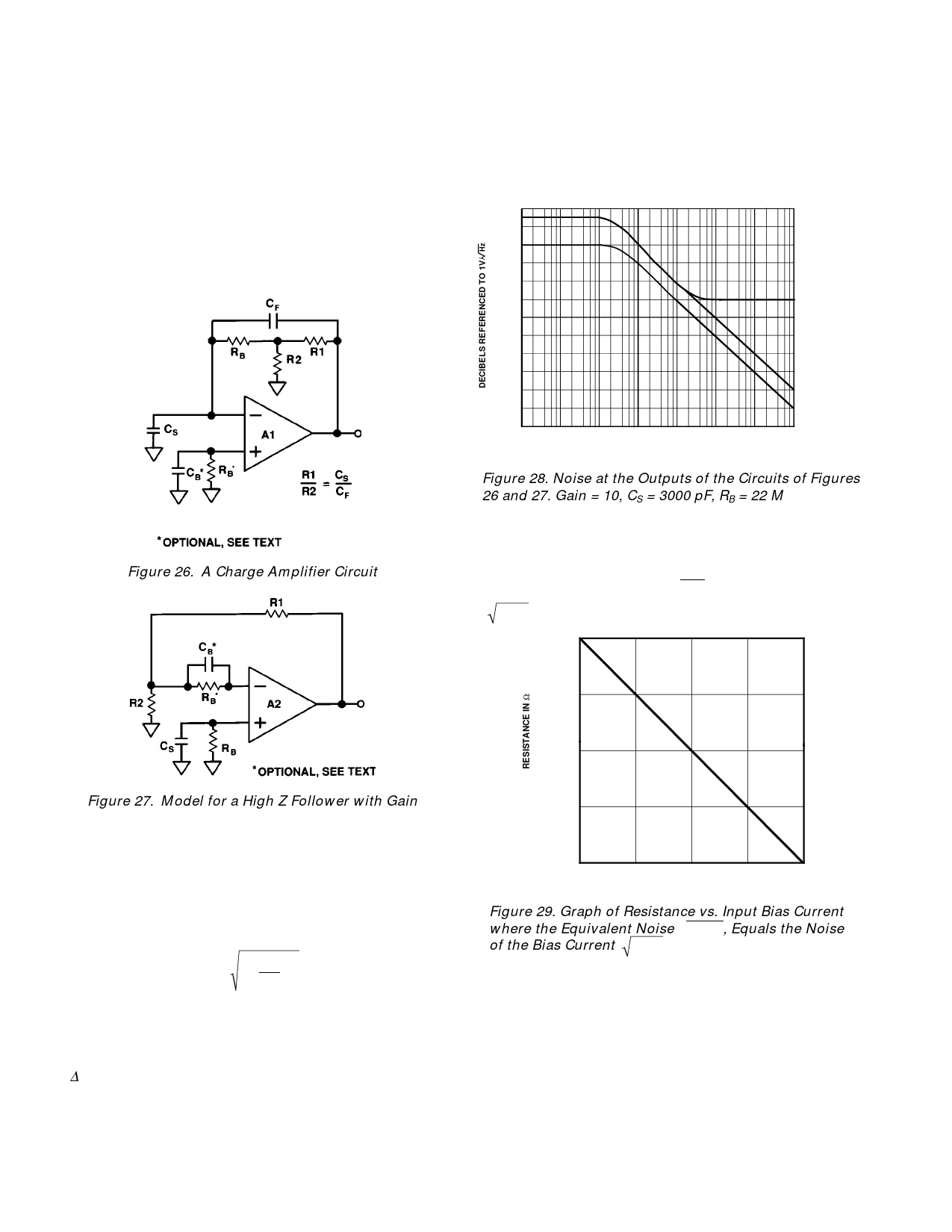
Figures 26 and 27 show two ways to buffer and amplify the
output of a charge output transducer. Both require using an
amplifier which has a very high input impedance, such as the
AD743. Figure 26 shows a model of a charge amplifier circuit.
Here, amplification depends on the principle of conservation of
charge at the input of amplifier A1, which requires that the
charge on capacitor CS be transferred to capacitor CF, thus
yielding an output voltage of ∆Q/CF. The amplifiers input
voltage noise will appear at the output amplified by the noise
gain (1 + (CS/CF)) of the circuit.
Figure 26. A Charge Amplifier Circuit
Figure 28 shows that these two circuits have an identical
frequency response and the same noise performance (provided
that CS/CF = R1/ R2). One feature of the first circuit is that a
“T” network is used to increase the effective resistance of RB
and improve the low frequency cutoff point by the same factor.
–100
–110
–120
–130
–140
–150
–160
–170
–180
–190
–200
–210
–220
10M
100M
1
10
100
1k
FREQUENCY – Hz
TOTAL OUTPUT
NOISE
NOISE DUE TO
R B ALONE
NOISE DUE TO
IB ALONE
10k 100k
Figure 28. Noise at the Outputs of the Circuits of Figures
26 and 27. Gain = 10, CS = 3000 pF, RB = 22 MΩ
However, this does not change the noise contribution of RB
which, in this example, dominates at low frequencies. The graph
of Figure 29 shows how to select an RB large enough to minimize
this resistor’s contribution to overall circuit noise. When the
equivalent current noise of RB ((√4kT)/R) equals the noise of IB
( 2qIB ), there is diminishing return in making RB larger.
5.2 x 10¹⁰
5.2 x 10 9
5.2 x 10 8
Figure 27. Model for a High Z Follower with Gain
The second circuit, Figure 27, is simply a high impedance
follower with gain. Here the noise gain (1 + (R1/R2)) is the
same as the gain from the transducer to the output. Resistor RB,
in both circuits, is required as a dc bias current return.
There are three important sources of noise in these circuits.
Amplifiers A1 and A2 contribute both voltage and current noise,
while resistor RB contributes a current noise of:
~
N=
T
4k
∆f
RB
where:
k = Boltzman’s Constant = 1.381 x 10⁻²³ Joules/Kelvin
T = Absolute Temperature, Kelvin (0°C = +273.2 Kelvin)
∆f = Bandwidth – in Hz (Assuming an Ideal “Brick Wall”
Filter)
This must be root-sum-squared with the amplifier’s own current
noise.
5.2 x 10⁷
5.2 x 10 6
1pA
10pA
100pA
1nA
INPUT BIAS CURRENT
10nA
Figure 29. Graph of Resistance vs. Input Bias Current
where the Equivalent Noise √4kT/R, Equals the Noise
of the Bias Current 2qIB
To maximize dc performance over temperature, the source
resistances should be balanced on each input of the amplifier.
This is represented by the optional resistor RB in Figures 26 and
27. As previously mentioned, for best noise performance care
should be taken to also balance the source capacitance designated
by CB. The value for CB in Figure 26 would be equal to CS, in
Figure 27. At values of CB over 300 pF, there is a diminishing
impact on noise; capacitor CB can then be simply a large bypass
of 0.01 µF or greater.
–8–
REV. C
Share Link: 