AD7398 查看數據表(PDF) - Analog Devices
零件编号
产品描述 (功能)
生产厂家
AD7398 Datasheet PDF : 24 Pages
| |||
AD7398/AD7399
Parameter
AC CHARACTERISTICS
Output Slew Rate
Settling Time8
Shutdown Recovery
DAC Glitch
Digital Feedthrough
Feedthrough
SUPPLY CHARACTERISTICS
Shutdown Supply Current
Positive Supply Current
Negative Supply Current
Power Dissipation
Power Supply Sensitivity
Symbol
SR
tS
tSDR
Q
QDF
VOUT/VREF
IDD_SD
IDD
IDD
ISS
PDISS
PSS
Condition
Data = 000H to 3FFH to 000H
To ±0.1% of full scale
Code 1FFH to 200H to 1FFH
VREF = 1.5 VDC + 1 V p-p,
data = 000H, f = 100 kHz
No load
VIL = 0 V, no load,
−40°C < TA < +125°C
VIL = 0 V, no load,
−40°C < TA < +85°C
VIL = 0 V, no load
VIL = 0 V, no load
ΔVDD = ±5%
3 V to 5 V ± 10% ±5 V ± 10%
2
2
6
6
6
6
150
150
15
15
−63
−63
Unit
V/μs typ
μs typ
μs typ
nVs typ
nVs typ
dB typ
30/60
1.5/2.8
1.5/2.6
1.5/2.5
5
0.006
30/60
1.6/3
1.6/2.8
1.6/2.7
16
0.006
μA typ/max
mA typ/max
mA typ/max
mA typ/max
mW typ
%/% max
1 One LSB = VREF/1024 V for the 10-bit AD7399.
2 The first two codes (000H and 001H) are excluded from the linearity error measurement in single-supply operation.
3 These parameters are guaranteed by design and not subject to production testing.
4 When VREF is connected to either the VDD or the VSS power supply, the corresponding VOUT voltage programs between ground and the supply voltage minus the offset
voltage of the output buffer, which is the same as the VZSE error specification. See additional discussion in the Theory of Operation section.
5 Input resistance is code dependent.
6 Typicals represent average readings measured at 25°C.
7 All input control signals are specified with tR = tF = 2 ns (10% to 90% of 3 V) and timed from a voltage level of 1.5 V.
8 The settling time specification does not apply for negative going transitions within the last 3 LSBs of ground.
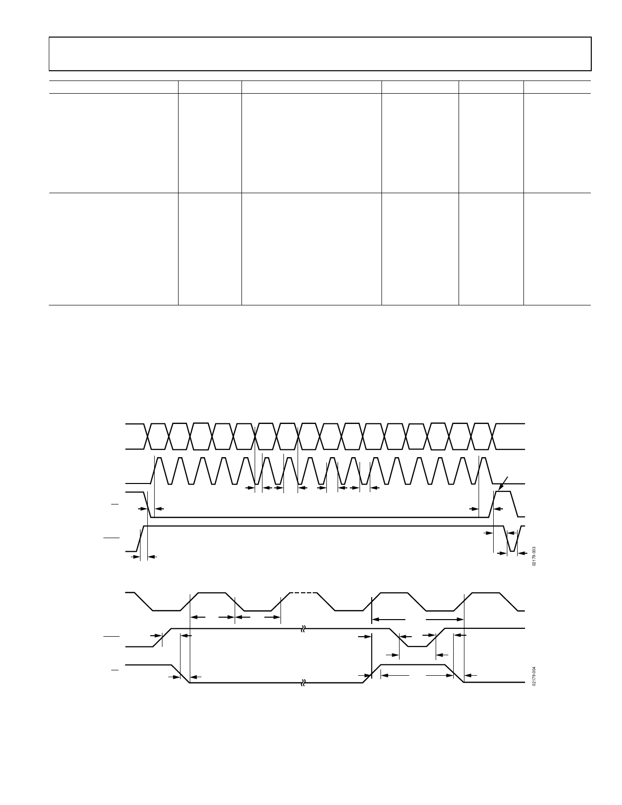
TIMING DIAGRAMS
SDI
SA SD A1 A0 D11 D10 D9 D8 D7 D6 D5 D4 D3 D2 D1 D0
CLK
CS
LDAC
tCSS
tLDS
tDS
tDH
tCH
tCL
Figure 3. AD7398 Timing Diagram (AD7399 with SDI = 14 Bits Only)
IN
REG
LD
tCSH
tLDH
tLDAC
CLK
LDAC
CS
tCH
tLDS
tCSS
tCL
tLDH
tCSH
Figure 4. Continuous Clock Timing Diagram
1/fCLK
tLDAC
tLDS
tCSS
Rev. C | Page 5 of 24
Share Link: 