AD7398 查看數據表(PDF) - Analog Devices
零件编号
产品描述 (功能)
生产厂家
AD7398 Datasheet PDF : 24 Pages
| |||
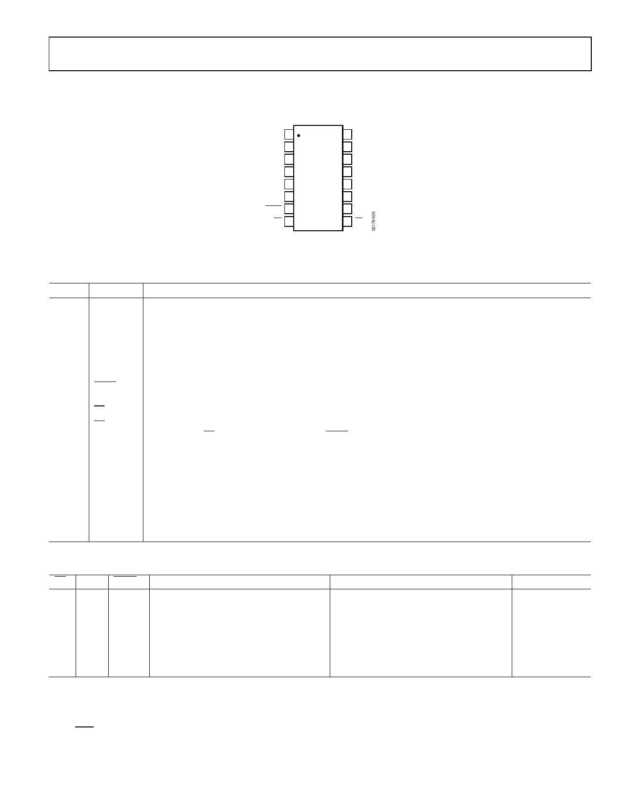
PIN CONFIGURATION AND FUNCTION DESCRIPTIONS
AD7398/AD7399
VOUTB 1
VOUTA 2
VSS 3
VREFA 4
VREFB 5
GND 6
16 VOUTC
AD7398/
AD7399
TOP VIEW
(Not to Scale)
15 VOUTD
14 VDD
13 VREFC
12 VREFD
11 SDI
LDAC 7
10 CLK
RS 8
9 CS
Figure 5. Pin Configuration
Table 4. Pin Function Descriptions
Pin No. Mnemonic Description
1
VOUTB
DAC B Voltage Output.
2
VOUTA
DAC A Voltage Output.
3
VSS
Negative Power Supply Input. Specified range of operation 0 V to −5.5 V.
4
VREFA
DAC A Reference Voltage Input Terminal. Establishes DAC A full-scale output voltage. Pin can be tied to VDD pin or VSS pin.
5
VREFB
DAC B Reference Voltage Input Terminal. Establishes DAC B full-scale output voltage. Pin can be tied to VDD pin or VSS pin.
6
GND
Ground Pin.
7
LDAC
Load DAC Register Strobe. Level sensitive active low. Transfers all input register data to DAC registers.
Asynchronous active low input. See Table 5 for operation.
8
RS
Resets Input and DAC Registers to All Zero Codes. Shift register contents unchanged.
9
CS
Chip Select. Active low input. Disables shift register loading when high. Transfers serial register data to the input
register when CS returns high. Does not effect LDAC operation.
10
CLK
Schmitt Triggered Clock Input. Positive edge clocks data into shift register.
11
SDI
Serial Data Input. Input data loads directly into the shift register.
12
VREFD
DAC D Reference Voltage Input Terminal. Establishes DAC D full-scale output voltage. Pin can be tied to VDD pin or VSS pin.
13
VREFC
DAC C Reference Voltage Input Terminal. Establishes DAC C full-scale output voltage. Pin can be tied to VDD pin or VSS pin.
14
VDD
Positive Power Supply Input. Specified range of operation 3 V to 5 V ± 10%.
15
VOUTD
DAC D Voltage Output.
16
VOUTC
DAC C Voltage Output.
Table 5. Control Logic Truth Table
CS CLK LDAC Serial Shift Register Function
HX
H
No effect
LL
H
No effect
L ↑+ H
LH
H
Shift register data advanced one bit
No effect
↑+ L/H H
No effect
HX
L
No effect
HX
↑+
No effect
Input Register Function
No effect
No effect
Latched
Latched
Updated with shift register contents
Latched
Latched
DAC Register
No effect
No effect
No effect
No effect
No effect
Transparent
Latched
NOTES
1. ↑+ = Positive logic transition; ↓– = Negative logic transition; X = Don’t Care.
2. At power-on, both the input register and the DAC register are loaded with all zeros.
3. During power shutdown, reprogramming of any internal registers can take place, but the output amplifiers do not produce the new values until the part is taken out
of shutdown mode.
4. The LDAC input is a level-sensitive input that controls the four DAC registers.
Rev. C | Page 7 of 24
Share Link: 