AD7398 查看數據表(PDF) - Analog Devices
零件编号
产品描述 (功能)
生产厂家
AD7398 Datasheet PDF : 24 Pages
| |||
AD7398/AD7399
INPUT REGISTERS
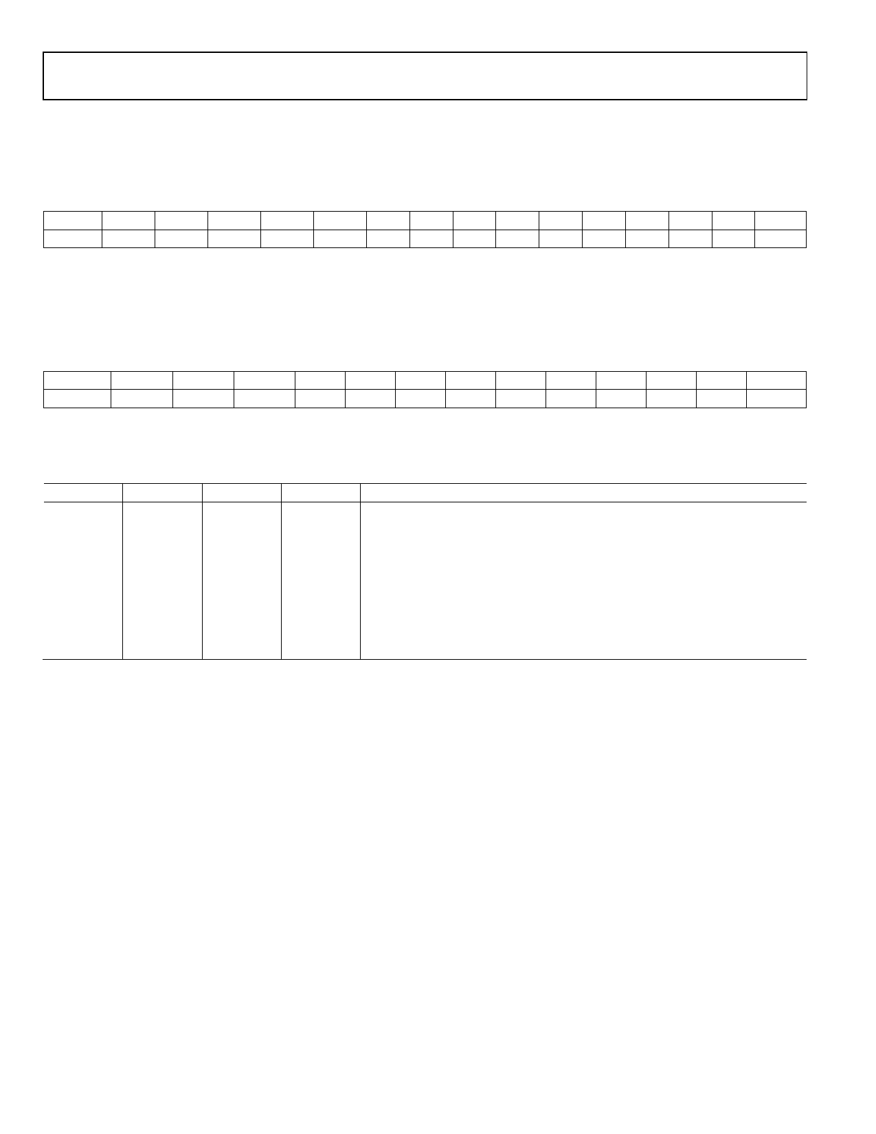
AD7398 SERIAL INPUT REGISTER DATA FORMAT
Data is loaded in the MSB first format.
MSB
LSB
B15
B14 B13 B12 B11 B10 B9 B8 B7 B6 B5 B4 B3 B2 B1 B0
SA
SD
A1
A0
D11 D10 D9 D8 D7 D6 D5 D4 D3 D2 D1 D0
NOTE
Bit Position B14 and Bit Position B15 are the SD and SA power shutdown control bits. If SA is set to Logic 1, all DACs are placed in the power shutdown mode. If SD is set
to Logic 1, the address decoded by Bit B12 and Bit B13 (A0 and A1) determine the DAC channel that is placed in the power shutdown state.
AD7399 SERIAL INPUT REGISTER DATA FORMAT
Data is loaded in the MSB first format.
MSB
B13
SA
B12
B11
SD
A1
LSB
B10
B9
B8
B7
B6
B5
B4
B3
B2
B1
B0
A0
D9
D8
D7
D6
D5
D4
D3
D2
D1
D0
NOTE
Bit Position B12 and Bit Position B13 are the SD and SA power shutdown control bits. If SA is set to Logic 1, all DACs are placed in the power shutdown mode. If SD is set
to Logic 1, the address decoded by Bit B10 and Bit B11 (A0 and A1) determine the DAC channel that is placed in the power shutdown state.
Table 6. AD7398/AD7399 Address Decode Control
SA
SD
A1
A0
1
X
X
X
0
1
0
0
0
1
0
1
0
1
1
0
0
1
1
1
0
0
0
0
0
0
0
1
0
0
1
0
0
0
1
1
DAC Channel Affected
All DACs shutdown
DAC A shutdown
DAC B shutdown
DAC C shutdown
DAC D shutdown
DAC A input register decoded
DAC B input register decoded
DAC C input register decoded
DAC D input register decoded
Rev. C | Page 8 of 24
Share Link: 