CXD2428Q 查看數據表(PDF) - Sony Semiconductor
零件编号
产品描述 (功能)
生产厂家
CXD2428Q Datasheet PDF : 16 Pages
| |||
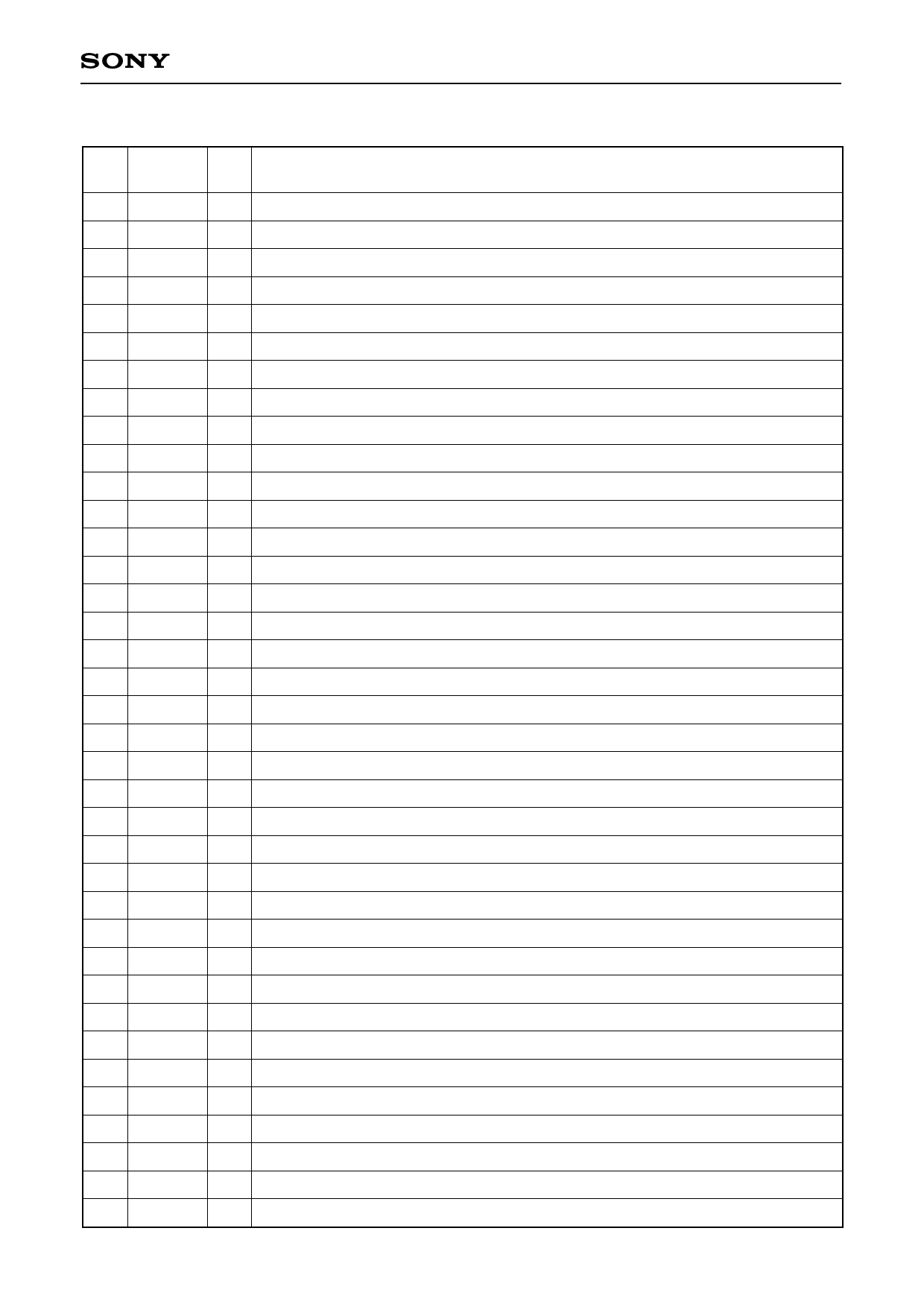
Pin Description
Pin
No.
Symbol
I/O
Description
1 SCLK
I Serial transfer clock
2 SCTR
I Serial transfer control
3 VDD0
— Power supply
4 VSS0
— GND
5 SDAT
I Serial transfer data
6 TST0
O Leave open.
7 P0
I/O I/O port
8 P1
I/O I/O port
9 P2
I/O I/O port
10 VBLK
O Vertical blanking output
11 TST1
I Fixed to high.
12 FSL1
I Field identification selection (High: internal, Low: external)
13 FSL2
I Field information polarity switching
14 TST2
I Fixed to low.
15 VSS1
— GND
16 BLNK
I Output data control (High: black display)
17 TST3
I Fixed to high.
18 TST4
I Leave open.
19 TST5
I Leave open.
20 VOUT
O Vertical sync signal output
21 HOUT
O Horizontal sync signal output
22 HBLK
O Horizontal blanking signal
23 CD7
O B-Y/R-Y data output (MSB)
24 CD6
O B-Y/R-Y data output
25 CD5
O B-Y/R-Y data output
26 CD4
O B-Y/R-Y data output
27 CD3
O B-Y/R-Y data output
28 VDD1
— Power supply
29 VSS2
— GND
30 CD2
O B-Y/R-Y data output
31 CD1
O B-Y/R-Y data output
32 CD0
O B-Y/R-Y data output (LSB)
33 YD7
O Y data output (MSB)
34 YD6
O Y data output
35 YD5
O Y data output
36 YD4
O Y data output
37 YD3
O Y data output
–3–
CXD2428Q
Share Link: 