GS4982CDA(1996) 查看數據表(PDF) - Gennum -> Semtech
零件编号
产品描述 (功能)
生产厂家
GS4982CDA Datasheet PDF : 7 Pages
| |||
BACK PORCH OUTPUT (pin 5)
In an NTSC composite video signal, horizontal sync pulses are
followed by the back porch interval. The GS4882 and GS4982
generate a negative going pulse on pin 5 during this time. It is
delayed typically 525 ns from the rising edge of sync and has
a typical width of 2.5 µs.
During the pre-equalizing, vertical sync and post equalizing
periods, composite sync doubles in frequency. The GS4882
and GS4982 maintain the back porch output at the horizontal
rate due to a Back Porch Enable (BPEN) signal, generated by
the internal Windowing Circuit, which forces back porch to be
output at the horizontal rate.
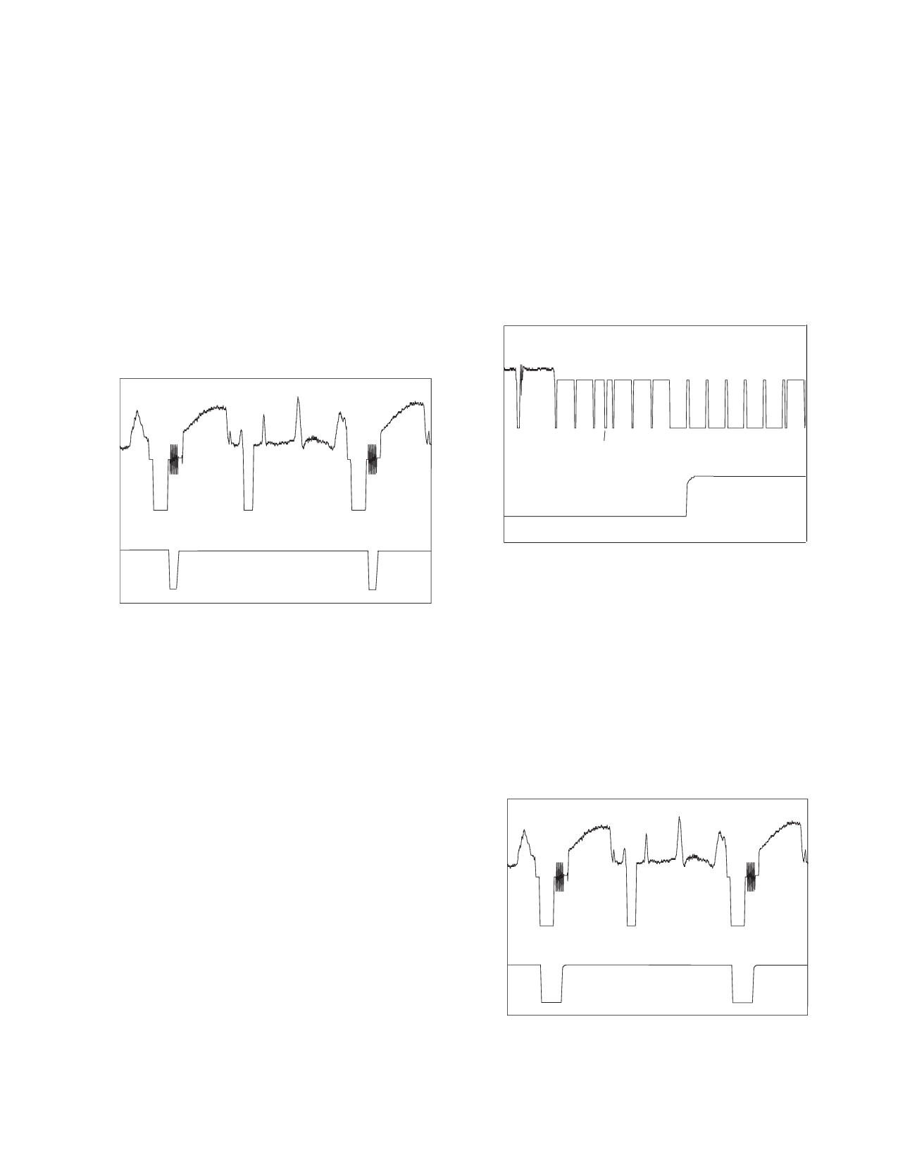
This gating circuit is also the reason for the excellent impulse
noise immunity of the back porch output as shown in Figure 3.
The GS4882 and GS4982 determine odd/even field information
by comparing vertical sync with an internally generated
horizontal sync. This output is clocked out by the falling edge
of vertical sync. The odd/even output is low during even fields
and high during odd fields.
This method of determining odd / even field information
provides for superior noise immunity. Noise during the pre-
equalizing pulses does not affect the output since the field
decision is made at the beginning of the vertical interval. This
noise immunity is displayed in Figure 4 in which an extra pre-
equalizing pulse has been added to the video input with no
negative effect on the odd/even field information.
Video
Input
Video
Input
Back
Porch
Output
Impulse
Noise
Odd / Even
Output
Impulse
Noise
Even
Odd
Fig. 4 Noise Immunity of Odd/Even Output
Fig. 3 Noise Immunity of Back Porch Output
VERTICAL SYNC OUTPUT (pin 3)
The vertical sync interval is detected by integrating the
composite sync pulses. The first broad pulse causes an
internal capacitor to charge past a fixed threshold and raises
an internal vertical flag. Once the vertical flag is raised, the
positive edge of the next serration clocks out the vertical
output. When the vertical sync interval ends, the first post
equalizing pulse is unable to charge the capacitor sufficiently,
causing the vertical interval flag to go high. The rising edge of
the second post-equalizing pulse then clocks out the high flag
to end the vertical sync pulse. The vertical output is clocked
in and out and therefore is a fixed width. Since the vertical
detector is designed as a true integrator, it provides improved
noise immunity.
ODD/EVEN OUTPUT (pin 7)
NTSC, PAL and SECAM composite video standards are
interlaced video schemes and therefore have odd and even
fields. For odd fields, the first broad vertical sync pulse is
coincident with the start of horizontal, while for even fields, the
first broad vertical sync pulse starts in the middle of a horizontal
line.
HORIZONTAL OUTPUT (pin 1 on GS4982)
As mentioned previously, the odd/even field output of the
device is generated by comparing vertical sync with an internal
horizontal sync signal. This horizontal sync signal is a true
horizontal signal (i.e. maintained during the vertical interval)
and is output on pin 1 of the GS4982. A delay of 420 ns and
a width of 8.0 µs are typical for this signal. The internal
Windowing Circuit which generates horizontal sync provides
excellent impulse noise immunity as shown in Figure 5.
Video
Input
Horizontal
Output
Impulse
Noise
Fig. 5 Noise Immunity of Horizontal Sync Output
521 - 61 - 00
4
Share Link: 