LC74793 查看數據表(PDF) - SANYO -> Panasonic
零件编号
产品描述 (功能)
生产厂家
LC74793 Datasheet PDF : 24 Pages
| |||
LC74793, 74793JM
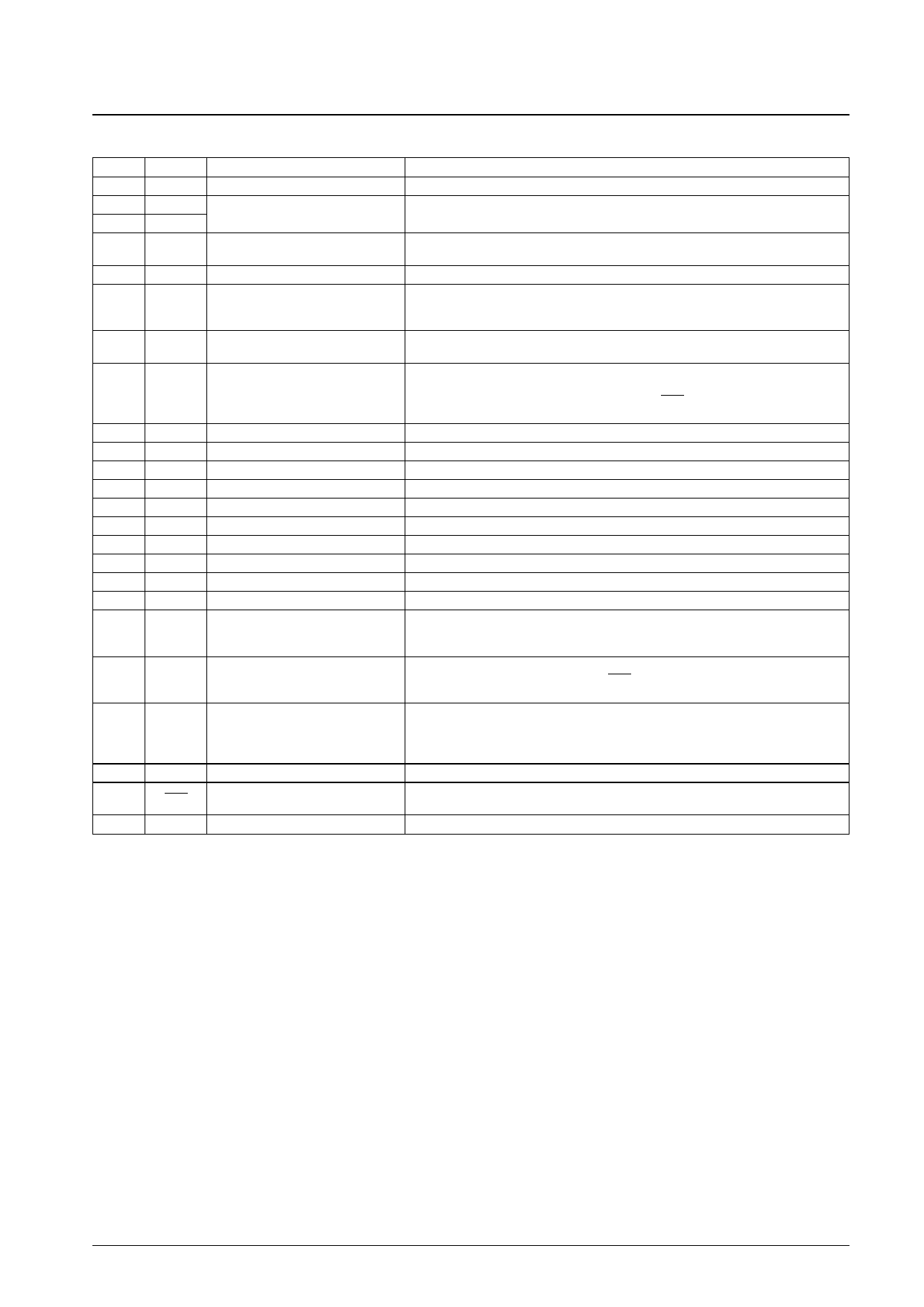
Pin Functions
Pin No.
1
2
3
4
5
6
7
8
9
10
11
12
13
14
15
16
17
18
19
20
21
22
23
24
Pin
Function
Description
VSS1
Xtalin
Xtalout
Ground
Crystal oscillator connections
Digital system ground
Connections for the crystal element and capacitors that form the crystal oscillator. Also
used for external clock input (fsc, 2fsc, or 4fsc).
CTRL1 Crystal element switching
Switches between external clock input mode and crystal oscillator mode. Set this pin low
for crystal oscillator, and high for external clock input.
NC
SDA
Data I/O
I2C bus
PDC/VPS data I/O.
I2C bus write address: 01111100
I2C bus read address: 01111101
SCL
Clock input
I2C bus
PDC/VPS data clock input.
I2C bus
External synchronizing signal
SYNCJDG discrimination output
External synchronizing signal presence/absence discrimination status output.
A high level is output when synchronizing signals are present.
This pin outputs the crystal oscillator clock when the RST pin is low.
(This reset state output can be disabled with command input.)
Hout Horizontal synchronizing signal output Horizontal synchronizing signal output
VSS2 Ground
Ground. (VCO circuit ground)
CPOUT
VCOIN
VCOR
Charge pump output
Oscillator control voltage input
Oscillator range adjustment
Charge pump output. Connect a low-pass filter to this pin.
VCO oscillation control voltage input
VCO oscillation range adjustment resistor connection
DAV Data acquisition output
Outputs a low level when PDC/VPS data has been discriminated
VDD2
SYNin
Power supply (+5 V)
Sync separator circuit input
Power supply (+5 V) (VCO system power supply)
Internal sync separator circuit video signal input
SEPC Slice level output
Slice level verification
SEPOUT
SEPIN
Composite synchronizing signal output Internal sync separator circuit composite synchronizing signal output
Vertical synchronizing signal input
Inputs the vertical synchronizing signal by integrating the SEP out pin output signal.
Applications must connect the SEP out pin to this pin through an integration circuit. If
unused, connect this pin to VDD1. (This pin is enabled when CTRL2 is high.)
Vout Vertical synchronizing signal output
Vertical synchronizing signal output
This pin outputs the VCO clock when the RST pin is low.
(This reset state output can be disabled with command input.)
CTRL2 SEPin input control
Controls whether or not the VSYNC vertical synchronizing signal is input to the SEPin
input.
When low: The VSYNC signal is not input. (The internal vertical separation circuit is used.)
When high: The VSYNC signal is input.
CDLR Clock phase adjustment
Connection for the clock phase adjustment resistor.
RST Reset input
System reset input.
A pull-up resistor is built in. (This input has hysteresis characteristics.)
VDD1 Power supply (+5 V)
Power supply. (+5 V: digital system power supply)
No. 5966-3/24
Share Link: 