SDA5650 查看數據表(PDF) - Infineon Technologies
零件编号
产品描述 (功能)
生产厂家
SDA5650 Datasheet PDF : 41 Pages
| |||
SDA 5650/X
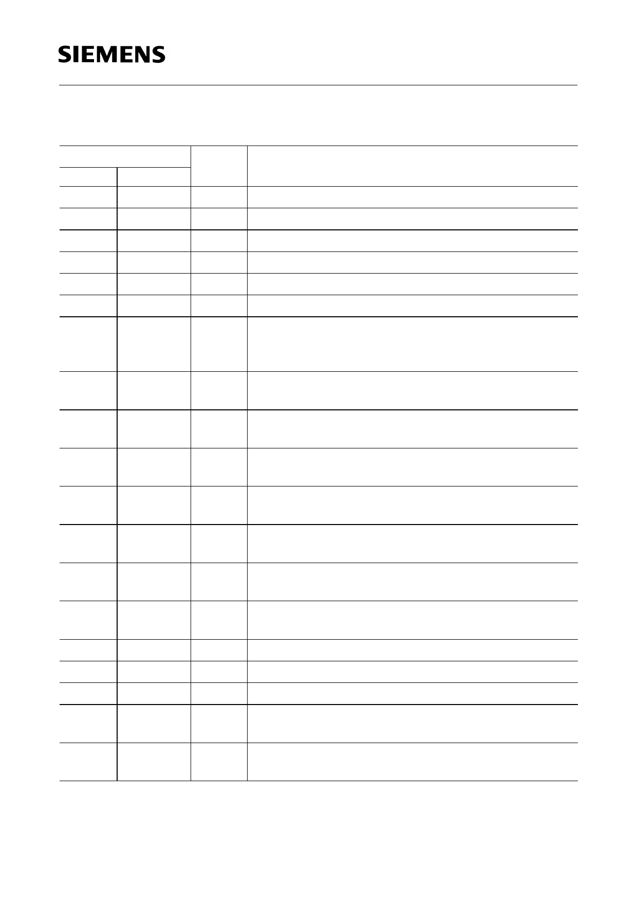
1.3 Pin Description
Pin No.
Symbol Function
P-DIP-14-1 P-DSO-20-1
1
VSS
Ground (0 V)
1
VSSA Analog ground (0 V)
2
VSSD Digital ground (0 V)
3, 8, 13, 18 N.C. Not connected
2
4
SCL Serial clock input of I2C Bus.
3
5
SDA Serial data input of I2C Bus.
4
6
5
7
CS0
VCS
Chip select input determining the I2C-Bus addresses:
20H / 21H, when pulled low
22H / 23H, when pulled high.
Video Composite Sync output from sync slicer used for
PLL based clock generation.
6
9
DAVN Data available output active low, when VPS data is
received.
7
10
EHB
Output signaling the presence of the first field active
high.
8
11
TI
Test input; activates test mode when pulled high.
Connect to ground for operating mode.
9
12
PD1 Phase detector/charge pump output of data PLL
(DAPLL).
10
14
PD2/ Connector of the loop filter for the SYSPLL.
VCO2
11
15
VCO1 Input to the voltage controlled oscillator #1 of the
DAPLL.
12
16
13
17
IREF Reference current input for the on-chip analog circuit.
CVBS Composite video signal input.
14
19
VDD
VDDD
Positive supply voltage (+ 5 V nom.).
Positive supply voltage for the digital circuits
(+ 5 V nom.).
20
VDDA Positive supply voltage for the analog circuits
(+ 5 V nom.).
Semiconductor Group
6
02.97
Share Link: 