RF2469 查看數據表(PDF) - RF Micro Devices
零件编号
产品描述 (功能)
生产厂家
RF2469 Datasheet PDF : 18 Pages
| |||
RF2469
Preliminary
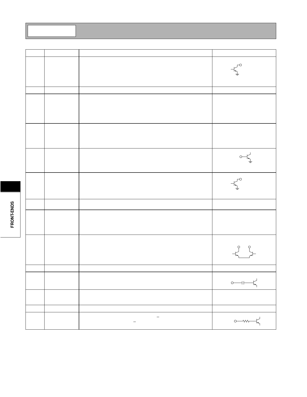
Pin Function Description
Interface Schematic
1
LNA1 OUT LNA output pin. This is an open-collector output. Externally matched to
50 Ω.
LNA1 OUT
2
GND
This pin is connected to the ground plane.
3
VCC1
Supply voltage for LNA1. An external resistor is placed in series with
this pin to adjust the current and IIP3 of LNA1. A nominal value of
1.1kΩ sets the LNA1 current to 4.5mA with a minimum IIP3 of +7dBm.
External RF bypassing is required. The trace length between the
bypass caps and the pin should be minimized. Connect ground sides of
caps directly to ground.
4
VCC1
Supply voltage for LNA2. An external resistor is placed in series with
this pin to adjust the current and IIP3 of LNA2. A nominal value of
2.4kΩ sets the LNA2 current to 1.6mA. External RF bypassing is
required. The trace length between the bypass caps and the pin should
be minimized. Connect ground sides of caps directly to ground.
5
LNA2 IN RF input to LNA2. This pin is internally DC-biased and, if it is con-
nected to a device with DC present, should be DC-blocked with a
capacitor suitable for the frequency of operation.
LNA2 IN
6
LNA2 OUT LNA output pin. This is an open-collector output. In normal operation,
this pin is externally cascaded with pin 8 (MIX IN).
8
LNA2 OUT
7
GND
Ground connection. For best performance, keep traces physically short
and connect directly to ground plane.
8
MIX IN
Mixer RF input pin. This pin requires a DC path to ground. In normal
operation, this pin is externally cascaded with pin 6 (LNA2 OUT). The
external match ensures a conjugate match between pin 6 and pin 8
while providing a DC path to ground for pin 8 and a DC-block between
pin 8 and pin 6.
9
IF+
IF output pin. The output is balanced. A current combiner external net-
work performs a differential to single-ended conversion and sets the
output impedance. There must be a DC path from VCC to this pin. This
is normally achieved with the current combiner network. A DC blocking
cap must be present if the IF filter input has a DC path to ground.
IF+
IF-
10
IF-
Same as pin 9, except complementary output.
See pin 9.
11
LO IN
Mixer LO single-ended input. The pin is internally DC-blocked. External
matching sets impedance.
LO IN
12
VCC1
Supply voltage for LO buffer. External RF bypassing is required. The
trace length between the bypass caps and the pin should be minimized.
Connect ground sides of caps directly to ground.
13
GND
This pin is connected to the ground plane.
14 LNA2 BYP Logic control for LNA2 gain. A logic high (>2.4V) places LNA2 in the
high gain mode. A logic low (<0.3V) place LNA2 in the bypass mode.
LNA2 BYP
32 kΩ
8-36
Rev A5 010717
Share Link: 