PBSS2515 查看數據表(PDF) - Philips Electronics
零件编号
产品描述 (功能)
生产厂家
PBSS2515 Datasheet PDF : 12 Pages
| |||
Philips Semiconductors
15 V low VCEsat NPN double transistor
Product specification
PBSS2515VS
FEATURES
• 300 mW total power dissipation
• Very small 1.6 x 1.2 mm ultra thin package
• Excellent coplanarity due to straight leads
• Low collector-emitter saturation voltage
• High current capability
• Improved thermal behaviour due to flat lead
• Replaces two SC-75/SC-89 packaged low VCEsat
transistors on same PCB area
• Reduces required PCB area
• Reduced pick and place costs.
QUICK REFERENCE DATA
SYMBOL
PARAMETER
VCEO
ICM
RCEsat
collector-emitter voltage
peak collector current
equivalent on-resistance
MAX. UNIT
15
V
1
A
<500 mΩ
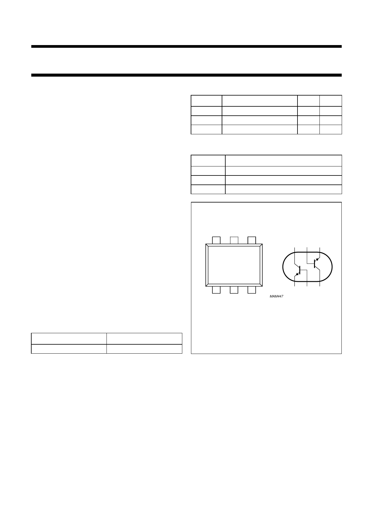
PINNING
PIN
1, 4
2, 5
6, 3
emitter
base
collector
DESCRIPTION
TR1; TR2
TR1; TR2
TR1; TR2
APPLICATIONS
• General purpose switching and muting
• Low frequency driver circuits
• LCD backlighting
handbook, halfpag6e
5
• Audio frequency general purpose amplifier applications
• Battery driven equipment (mobile phones, video
cameras and hand-held devices).
DESCRIPTION
NPN low VCEsat double transistor in a SOT666 plastic
package.
PNP complement: PBSS3515VS.
1
2
Top view
4
65 4
TR2
TR1
3
123
MAM447
MARKING
TYPE NUMBER
PBSS2515VS
MARKING CODE
N9
Fig.1 Simplified outline (SOT666) and symbol.
2001 Nov 07
2
Share Link: 