MAX888ECJ(1999) 查看數據表(PDF) - Maxim Integrated
零件编号
产品描述 (功能)
生产厂家
MAX888ECJ Datasheet PDF : 20 Pages
| |||
Wireless and Satellite Handset
Power-Management ICs
ABSOLUTE MAXIMUM RATINGS
BATT, IN0, IN1 to GND...........................................-0.3V to +13V
CVH to IN0................................................................-6V to +0.3V
PGND, DGND to GND...........................................-0.3V to +0.3V
ONSTAT to GND .....................................-0.3V to (VOUT2 + 0.3V)
LX to PGND.............................................-0.3V to (VOUT0 + 0.3V)
OUT1 to GND.............................................-0.3V to (VIN1 + 0.3V)
OUT2 to GND.............................................-0.3V to (VIN2 + 0.3V)
OUT3 to GND.............................................-0.3V to (VIN3 + 0.3V)
OUT5 to GND.............................................-0.3V to (VIN5 + 0.3V)
SYNC, RESET, SCL, SDA, CVL, LBI, LBHYS, OUT0
REF, LBO, C+, C-, OUT4, IN2, IN3, IN4, IN5,
ON, OFF to GND ...................................................-0.3V to +6V
Continuous Power Dissipation (TA = +70°C)
TQFP (derate 11.1mW/°C above +70°C) ......................889mW
Operating Temperature Range. ......................... -40°C to +85°C
Junction Temperature ......................................................+150°C
Storage Temperature Range .............................-65°C to +150°C
Lead Temperature (soldering, 10sec) .............................+300°C
Stresses beyond those listed under “Absolute Maximum Ratings” may cause permanent damage to the device. These are stress ratings only, and functional
operation of the device at these or any other conditions beyond those indicated in the operational sections of the specifications is not implied. Exposure to
absolute maximum rating conditions for extended periods may affect device reliability.
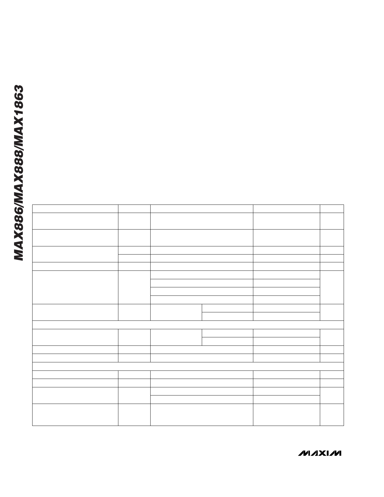
ELECTRICAL CHARACTERISTICS
(VBATT = VIN0 = VIN1 = +5.5V, GND = PGND = DGND, V OFF = VSYNC = 2.8V, VIN2 = VIN3 = VIN4 = VIN5 = +3.8V, VOUT4 = +5.5V,
TA = -40°C to +85°C, unless otherwise noted. Typical values are at TA = +25°C.) (Note 1)
PARAMETER
SYMBOL
CONDITIONS
MIN TYP MAX UNITS
BATT, IN0, IN1 Operating Voltage VBATT, VIN0,
Range
VIN1
2.7
12
V
IN2, IN3, IN4, IN5 Operating
Voltage Range
VIN2, VIN3,
VIN4, VIN5
2.7
5.5
V
Undervoltage Lockout
Supply Current, PFM Mode
VUVLOF
VUVLOR
IBATTPFM
VBATT falling
VBATT rising
SYNC = GND
2.35 2.45
V
2.55 2.65
V
250
600
µA
fOSC = 375kHz
2
Supply Current, PWM Mode
IBATTPWM fOSC = 535kHz
fOSC = 670kHz
3
mA
4
fOSC = 925kHz
5.5
12
Supply Current, Shutdown Mode
ISTNBY OFF = GND
TA = 0°C to +85°C
TA = -40°C to +85°C
5
10
µA
15
REFERENCE
Reference Output Voltage
VREF
IREF = 0
TA = 0°C to +85°C 1.23 1.25 1.27
V
TA = -40°C to +85°C 1.225
1.275
Reference Load Regulation
1µA < IREF < 100µA
5
15
mV
Reference Supply Rejection
2.7V < VOUT0 < 3.75V
0.2
5
mV
DC-DC BUCK REGULATOR 0 (IN0, OUT0)
Input Voltage Range
VIN0
2.7
12
V
Output Accuracy
IOUT0 = 0
-3
3
%
Nominal Output Adjustment
Range
VOUT0
MAX886
MAX888
2.625
1.527
3.750
V
3.027
Output Ready Threshold
VOUT0 = 3.75V (MAX886),
VOUT0 = 2.027V (MAX888)
-7.5
-5
-3
% of
VOUT0
2 _______________________________________________________________________________________
Share Link: 