DT28F320S5-90 查看數據表(PDF) - Intel
零件编号
产品描述 (功能)
生产厂家
DT28F320S5-90 Datasheet PDF : 50 Pages
| |||
28F160S5, 28F320S5
E
Individual block locking uses a combination of block
lock-bits to lock and unlock blocks. Block lock-bits
gate block erase, full chip erase, program and write
to buffer operations. Lock-bit configuration
operations (Set Block Lock-Bit and Clear Block
Lock-Bits commands) set and clear lock-bits.
The Status Register and the STS pin in RY/BY#
mode indicate whether or not the device is busy
executing an operation or ready for a new
command. Polling the Status Register, system
software retrieves WSM feedback. STS in RY/BY#
mode gives an additional indicator of WSM activity
by providing a hardware status signal. Like the
Status Register, RY/BY#-low indicates that the
WSM is performing a block erase, program, or lock-
bit operation. RY/BY#-high indicates that the WSM
is ready for a new command, block erase is
suspended (and program is inactive), program is
suspended, or the device is in deep power-down
mode.
The BYTE# pin allows either x8 or x16 read/writes
to the device. BYTE# at logic low selects 8-bit
mode with address A0 selecting between the low
byte and high byte. BYTE# at logic high enables
16-bit operation with address A1 becoming the
lowest order address. Address A0 is not used in 16-
bit mode.
When one of the CEX# pins (CE0#, CE1#) and RP#
pins are at VCC, the component enters a CMOS
standby mode. Driving RP# to GND enables a deep
power-down mode which significantly reduces
power consumption, provides write protection,
resets the device, and clears the Status Register. A
reset time (tPHQV) is required from RP# switching
high until outputs are valid. Likewise, the device
has a wake time (tPHEL) from RP#-high until writes
to the CUI are recognized.
1.3 Pinout and Pin Description
The Automatic Power Savings (APS) feature
substantially reduces active current when the
device is in static mode (addresses not switching).
The 16-Mbit device is available in the 56-lead
TSOP and 56-lead SSOP. The 32- Mb device is
available in the 56-lead SSOP. The pinouts are
shown in Figures 2 and 3.
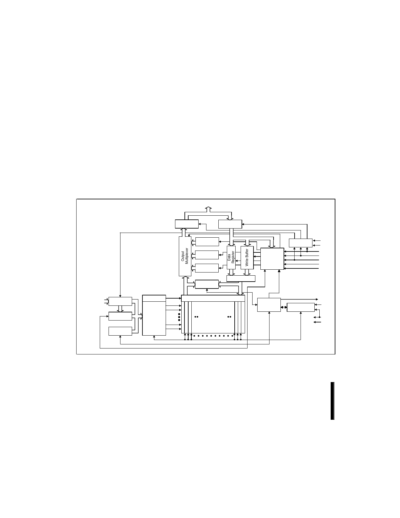
DQ0 - DQ15
16-Mbit: A0- A20
32-Mbit: A0 - A21
Input Buffer
Address
Latch
Address
Counter
Y-Decoder
X-Decoder
Output Buffer
Input Buffer
Query
Identifier
Register
Status
Register
Data
Comparator
Y-Gating
Multiplexer
16-Mbit: Thirty-two
32-Mbit: Sixty-four
64-Kbyte Blocks
Command
User
Interface
I/O Logic
VCC
BYTE#
CE#
WE#
OE#
RP#
WP#
Write State
Machine
Program/Erase
Voltage Switch
STS
VPP
VCC
GND
Figure 1. 28F320S5 and 28F160S5 Block Diagram
0608_01
6
ADVANCE INFORMATION
Share Link: 