SPT2210SCT 查看數據表(PDF) - Signal Processing Technologies
零件编号
产品描述 (功能)
生产厂家
SPT2210SCT Datasheet PDF : 22 Pages
| |||
Register Write:
After completing address setup, set CS_ low, RS
high.
Set the data required onto the data bus, then set WR_
low and then back high; this will write the Y data.
Set the data required onto the data bus, then set WR_
low and then back high; this will write the Cr data.
Set the data required onto the data bus, then set WR_
low and then back high; this will write the Cb data.
Set WR_, CS_ and RS high, then release data bus
input data.
This completes the three-byte sequence of the CLUT
register write operation at the specified address.
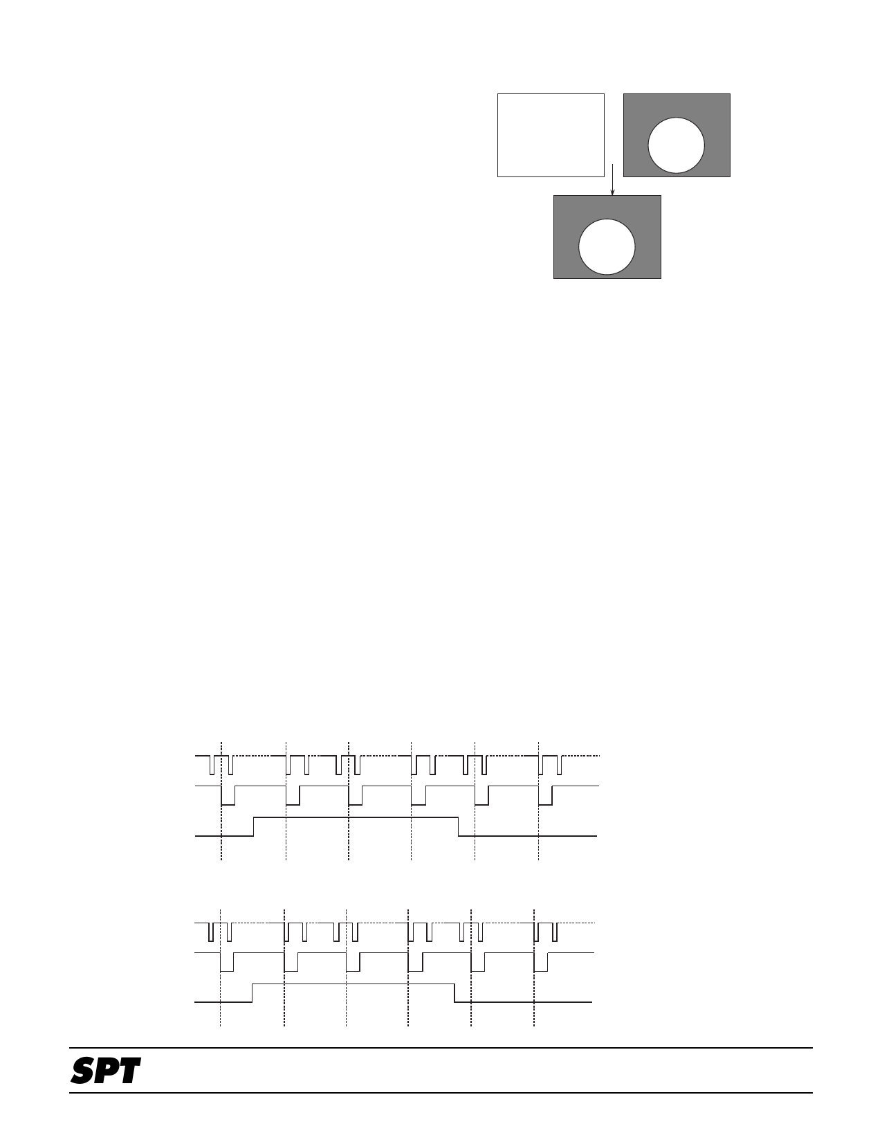
Figure 6 – Multiplex in Chroma Mode
GD3…0 (Except
transparent color)
YD7…0, CD7…0 +
GD3…0
(Transparent)
GD3…0
YD7…0
CD7…0
COMBINING VIDEO AND
GRAPHICS SIGNALS
EXTERNAL KEY MODE
The external key mode is selected by setting the com-
mand register CR1, bits D1...0 = 11 (binary). In this mode
it is possible to combine the video signals (YD7...0,
CD7...0) with the graphics signals (GD3...0). When the
KEY pin is high, in conformity with the timing shown in
figure 8, the graphics signals (out of the CLUT and refer-
enced by GD3...0) are output (i.e., displayed). This can
be done on a pixel-by-pixel basis.
VERTICAL INTERPOLATION
The SPT2210 has a vertical interpolation filter that is
used to reduce jaggy noise and flicker. It also supports
the high resolution mode for Video CD, version 2.0.
INTERPOLATION FIELD SELECTION
The vertical interpolation filter is active for each odd or
even field as specified in command register CR3, bit D3.
However, vertical interpolation is not active for NTSC line
21 and PAL line 25 when the ODD field is selected (CR3,
bit D3 = 0) and NTSC line 285 and PAL line 336 when the
EVEN field is selected (CR3, D3 = 1).
CHROMA MODE
The chroma key mode is selected by setting the com-
mand register CR1, bits D1...0 = 10 (binary). In this mode
the graphics signal image becomes the front image, and
the Y/C image becomes the rear image. The Y/C image is
displayed in the portions of the display in which the trans-
parent colors are specified in the graphics image data
stream. Figure 6 illustrates the combining of video and
graphics images in the chroma mode.
INTERPOLATION BYPASS
Vertical interpolation is automatically enabled and dis-
abled for the proper even/odd field depending on the field
selection specified in CR3, bit D3. The VRTENB pin en-
ables interpolation, in conjunction with the even/odd field
algorithm, as shown in figures 7 and 8. The interpolation
filter may be bypassed altogether by setting bit D2 in
command register CR3 or setting the VRTENB pin to
logic low.
Figure 7 – Vertical Interpolation Timing CR3 D2=0, D3=1; Even Field
Even
Odd
Even
Odd
Even
Odd
HSYNC_
VSYNC_
VRTENB
Vertical Interpolation Bypass
Bypass Active
Bypass Bypass
Bypass
Figure 8 – Vertical Interpolation Timing CR3 D2=0, D3=0; Odd Field
Even
Odd
Even
Odd
Even
Odd
HSYNC_
VSYNC_
VRTENB
Vertical Interpolation Bypass
Active
Bypass
Active
Bypass
Bypass
SPT
SPT2210
16
8/22/00
Share Link: 