SPT2210SCT 查看數據表(PDF) - Signal Processing Technologies
零件编号
产品描述 (功能)
生产厂家
SPT2210SCT Datasheet PDF : 22 Pages
| |||
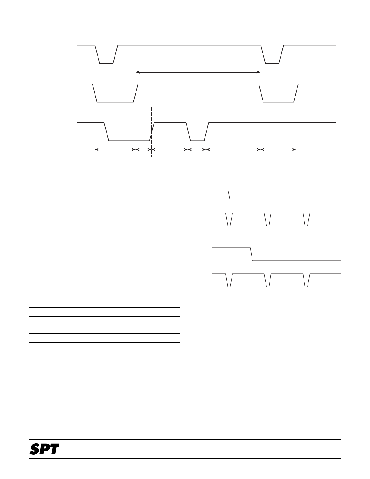
Figure 3 – Set of BLANK_ Terminal and Display/Nondisplay
HSYNC_
Internal Blank
Blank_
Nondisplay Non- Display
display
Non-
display
Display
Nondisplay
Blank_ Pin
This is the input pin for the external blanking control sig-
nal (TTL level). The SPT2210 samples BLANK_ at the
rising edge of CLK. When BLANK_ is high, the output
proceeds with normal operation and when it is low the
output signal gets blanked (i.e., no display). The specifi-
cation of the blank state can be performed on a pixel-by-
pixel basis.
The chip has an internal blanking function that operates
independent of the external blanking signal. Figure 3
shows operation of the internal blanking in conjunction
with external blanking. Table III delineates the internal
blanking that is generated regardless of the level of the
blank pin, upon detection of HSYNC_.
Figure 4 – Sync Signal Input Timing
VSYNC_
HSYNC_
VSYNC_
Odd Numbered Field
HSYNC_
Table III – Internal Blanking Periods for NTSC and
PAL
Lines
Lines
Line(s)
NTSC
1 to 20
263 to 283
525
PAL
1 to 23
310 to 335
623 to 625
V Pin
This input pin provides the timing to generate the vertical
signal out of the SPT2210. The mode of operation for this
pin is controlled by Command Register, CR5. The sam-
pling of the sync signal occurs on the rising edge of clock.
When the Vsync input signal is asserted during an Hsync
signal the field is considered to be odd, else the field is
even. (Refer to figure 4.)
When in the blank operational mode the field is deter-
mined by the field input signal.
Even Numbered Field
H Pin
This input pin provides the timing to generate the horizon-
tal signal out of the SPT2210. The mode of operation for
this pin is controlled by Command Register, CR5. The
sampling of the sync signal occurs on the rising edge of
clock. When the timing for Hsync/Hblank input is different
from the number of clock cycles shown in table IV, the
phase of the subcarrier will be put into free-run.
Since the horizontal blanking period in Figure 2 is deter-
mined internally, the width and the trailing edge of
HSYNC_ are not detected. The active pixels are output
after the completion of the back porch as shown in
figure 2.
SPT
SPT2210
5
8/22/00
Share Link: 